Germanium Sulfide (GeS) Powder and Crystals
More 2D Materials
We stock a wide range of 2D materials available to purchase online. Please contact us if you cannot find what you are looking for.
Germanium sulfide (GeS), CAS number 12025-32-0, is a group IV layered monochalcogenide with a similar atomic puckered structure to black phosphorus (BP) and a bandgap in the visible region (1.65 – 1.8 eV). Like BP, it has anisotropic optical properties, with low energy optical excitations along the armchair and zigzag directions. The anisotropic crystal structure of GeS gives rise to anisotropy in the optoelectronic properties, such as polarized optical absorption, photoconductivity.
High Purity
High purity Germanium Sulfide ≥99.995% powder
Worldwide Shipping
Quick and reliable shipping
Low Price
Low price Germanium Sulfide
Different Forms
Available in powder and crystals
With a bandgap of 1.65 eV, GeS as a layered semiconductors with a distorted rock-salt orthorhombic structure and a p-type semiconductor, is considered to be a promising photovoltaic material for high-efficiency solar cell and photodetectors with high sensitivity and external quantum efficiency. Nanoparticles, nanosheets, nanoflowers and nanowires of GeS with unique structures and physical properties have been developed for different applications.
Germanium selenide (GeSe) Powder from Ossila was used in the high-impact paper (IF 11.19), γ-GeSe: A New Hexagonal Polymorph from Group IV–VI Monochalcogenides, S. Lee et al., Nano Lett. 21, 4305–4313 (2021); DOI: 10.1021/acs.nanolett.1c00714.
Also with an indirect band gap of 2.34 eV which can be further fine tuned by external strain, GeS monolayer is semiconducting and its monolayer has an electron mobility of 3,680 cm2 V−1 s−1, much higher than that of MoS2 monolayer. GeS monolayers have been mostly been fabricated by mechanical and chemical exfoliations from bulk crystals or high-purity powders. Structurally pristine with minimal chemical degradation sub-10 nm thick GeS nanosheets can be achieved with liquid-phase exfoliation (LPE) in anhydrous N-methyl-2-pyrrolidone (NMP).
We supply low price Germanium sulfide in several different forms for a range of applications.

Germanium Sulfide Powder
Can be used for preparation of germanium sulfide nanoplates and ultrathin films
Sold by weight
≥99.995% purity
From £220

Germanium Sulfide Crystals by Size
Can be used to produce single or few-layer germanium sulfide sheets via mechanical or liquid exfoliation
Small (≥10 mm2) or medium (≥25 mm2) crystals available*
≥99.999% purity
From £520
*Typical representative size, areas/dimensions may vary
Bulk single Germanium sulfide crystal is most commonly used as sources from which single or few-layer sheets can be obtained via either mechanical or liquid exfoliation.
High purity germanium sulfide powder can also be used to prepare GeS nanosheets and nanoparticles by liquid-exfoliation (normally assisted by sonication).
Technical Data
| CAS Number | 12025-32-0 |
| Chemical Formula | GeS |
| Molecular Weight | 104.71 g/mol |
| Bandgap | 1.65 eV (indirect) |
| Preparation | Synthetic - Chemical Vapor Transport (CVT) |
| Structure | Orthorhombic |
| Electronic Properties | 2D semiconductor |
| Melting Point | 615 °C (lit) |
| Color | Dark grey |
| Synonyms | Germanium(II) sulfide, Germanium monosulfide |
| Classification / Family | Transition metal monochalcogenides (TMDCs), 2D semiconductor materials, Nano-electronics, Nano-photonics, Photovoltaic, Materials science |
Product Details
| Form | Purity |
|---|---|
| Powder | ≥99.995% |
| Crystal | ≥99.999% |
Pricing Table
| Product Code | Form | Size/Weight* | Price |
|---|---|---|---|
| M2303C1 | Powder | 500 mg | £220 |
| M2303C1 | Powder | 1 g | £350 |
| M2303A10 | Crystal | Small (≥10 mm2) | £520 ea. |
| M2303A25 | Crystal | Medium (≥25 mm2) | £850 ea. |
*typical representative size, areas/dimensions may vary
Shipping is free for qualifying orders.
MSDS Documents
Structure of Germanium Sulfide
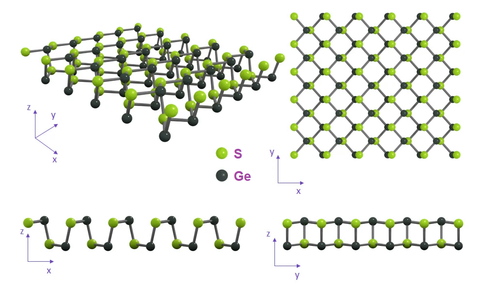
Germanium sulfide (GeS) belongs to the Group IV layered metal mono-chalcogenides. It is a layered material with structure analogous to that of black phosphorus. GeS crystallizes in a layered structure of distorted orthorhombic symmetry of space group Pcmn - D2h16. Bulk GeS has a unique structural characteristic with a puckered configuration along the x (armchair) direction and a bilayer structure along the y (zigzag) direction. Each of the monolayers stack along the z-axis and the unit cell comprises two adjacent double layers.
GeS orthorhombic form (also called α-GeS) has been proven to be dynamically and thermally stable at room temperature.

Literature and Reviews
- Ultrahigh drive current and large selectivity in GeS selector, S. Jia et al., Nat . Commun., 11, 4636 (2020); DOI: 10.1038/s41467-020-18382-z.
- Polarized Band-Edge Emission and Dichroic Optical Behavior in Thin Multilayer GeS, C-H. Ho et al., dv. Optical Mater., 5, 1600814 (2017); DOI: 10.1002/adom.20160081.
- Anisotropic optical and electronic properties of two dimensional layered germanium sulfide, D.Tan et al., Nano Res. 10, 546–555 (2017); DOI: 10.1007/s12274-016-1312-6.


