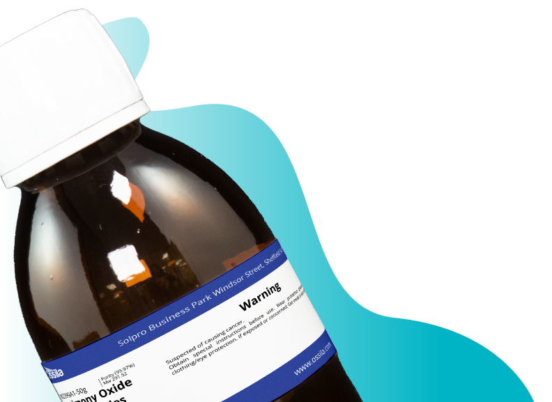
Tin(IV) Sulfide (SnS2) Powder and Crystal
Low price, high purity 2D metal tin(IV) sulfide powder and crystals
For the development of next-generation electronics, optoelectronics, and nanotechnology
Technical Data | MSDS | Structure | Literature and Reviews | Related Products | Resources | Technical Support
Tin(IV) sulfide (also known as tin disulfide SnS2), CAS number 1315-01-1, is a layered metal dichalcogenide semiconductor with a similar chemical and crystal structure to that of molybdenum disulfide (MoS2). In each individual layer, Sn is sandwiched between two S layers with strong covalent bonding, whereas individual mono-layers are held by weak van der Waals forces. Individual layers break free when weak van der Waals forces are overcome by either physical or chemical exfoliation.
Like many other two dimensional semiconductors, SnS2 can undergo exfoliation to form atomic-layer sheets that have applications in FETs, photovolatic solar cells, sensors and photocatalyst applications.
SnS2 is an n-type semiconducting material that has a hexagonal CdI2-type structure. It has attracted increasing attention as a promising anode materials due to its high theoretical capacity and abundancy.
High Purity
≥99.999% Crystal Purity
Worldwide Shipping
Quick and reliable shipping
Low Cost
Low Cost Tin(IV) Sulfide
Powder & Crystal
Different Forms of Tin(IV) Sulfide
We supply low price tin(IV) sulfide in several different forms for a range of applications.
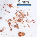
Tin(IV) Sulfide Powder
Can be used for preparation of tin(IV) sulfide nanoplates and ultrathin films
Sold by weight
≥99.995% purity
From £220
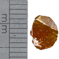
Tin(IV) Sulfide Crystals by Size
Can be used to produce single or few-layer tin(IV) sulfide sheets via mechanical or liquid exfoliation
Small (≥10 mm2) or medium (≥25 mm2) crystals available*
≥99.999% purity
From £520
*Typical representative size, areas/dimensions may vary
Bulk single tin(IV) sulfide crystal is most commonly used as sources from which single or few-layer sheets can be obtained via either mechanical or liquid exfoliation.
Tin(IV) sulfide powder can also be used to prepare SnS2 nanosheets and nanoparticles by liquid-exfoliation (normally assisted by sonication). Cu intercalated bilayer SnS2 displays a hole field-effect mobility of ~40 cm2 V−1 s−1, and Co-SnS2 exhibits a metal-like behavior with sheet resistance comparable to that of few-layer graphene.
Technical Data
| CAS Number | 1315-01-1 |
| Chemical Formula | SnS2 |
| Molecular Weight | 182.83 g/mol |
| Bandgap | 2.2 eV |
| Preparation | Synthetic - Chemical Vapor Transport (CVT) |
| Structure | Hexagonal (2H) |
| Electronic Properties | 2D CDW materials |
| Melting Point | N/A |
| Color | Dark brown |
| Synonyms | Tin disulfide, Stannic sulfide, Tin sulfide (S2Sn), Mosaic gold |
| Classification / Family | Transition metal dichalcogenides (TMDCs), 2D semiconductor materials, NIR band-gap, Nano-electronics, Nano-photonics, Transistors, Photovoltaics, Materials science |
Product Details
| Form | Purity |
|---|---|
| Powder | ≥99.995% |
| Crystal | ≥99.999% |
Pricing Table
| Product Code | Form | Size/Weight* | Price |
|---|---|---|---|
| M2114C1 | Powder | 500 mg | £220 |
| M2114C1 | Powder | 1 g | £350 |
| M2114A10 | Crystal | Small (≥10 mm2) | £520 ea. |
| M2114A25 | Crystal | Medium (≥25 mm2) | £850 ea. |
| M2114A00 | Crystal | Large (≥100 mm2) | £1800 ea. |
*Typical representative size, areas/dimensions may vary
Shipping is free for qualifying orders.
MSDS Documents
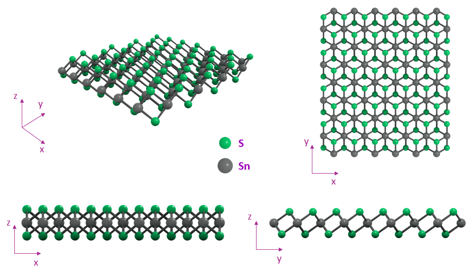
Structure of Tin(IV) Sulfide
Tin(IV) sulfide (SnS2) has a layered structure, where each Sn ion coordinates to six S ions in a regular octahedron. Each sheet of Sn atoms is sandwiched between two sheets of S atoms, and each S-Sn-S layer is held by weak van de Vaals interactions.
SnS2 crystallizes with a standard hexagonal crystal structure (2H-SnS2) which is identical to that of 1T-MoS2. Monolayers of 2H-SnS2 are stacked precisely on top of one another to form the 2H-polytype of bulk SnS2. It is noted that the 2H-SnS2 structure is different from that of 2H-MoS2, where the Mo atom possesses a trigonal prismatic coordination instead.
Literature and Reviews
- Tin Disulfide—An Emerging Layered Metal Dichalcogenide Semiconductor: Materials Properties and Device Characteristics, Y, Huang et al., ACS Nano, 8 (10), 10743–10755 (2014); DOI: 10.1021/nn504481r.
- Low-Frequency Raman Spectroscopy of Few-Layer 2H-SnS2, T. Sriv et al., Sci. Rep., 8 10194 (2018); DOI:10.1038/s41598-018-28569-6.
- Effect of strain on electronic and magnetic properties of Fe-doped monolayer SnS2, Y. Liu et al., Phy. Lett. A, 381, 1732–1737 (2017); DIO: 10.1016/j.physleta.2017.03.034.
Related Products
We stock a wide range of 2D materials available to purchase online. Please contact us if you cannot find what you are looking for.