Indium(II) Selenide (InSe) Powder and Crystal
Low price, high purity indium(II) selenide powder and crystals
Suitable for use a semiconductor, photoconductor, and in non-linear optics
Technical Data | MSDS | Structure | Literature and Reviews | Related Products | Resources and Support
Indium(II) selenide (InSe), CAS number 1312-42-1, belongs to the IIIA−VIA family group of 2D layered semiconductors. Each of its layers has a honeycomb lattice made of indium and selenium atoms.
High Purity
High purity ≥99.999% indium(II) selenide Crystal
Worldwide shipping
Quick and reliable shipping
Low price
Low price Indium(II) Selenide (InSe)
Powder & Crystal
Available in Powder & Crystal forms
Like black phosphorus (BP) - but with a much more stable nature under ambient conditions, ultra-thin indium selenide (InSe) offers a useful middle ground between silicon and graphene. Weak van der Waals forces between layers of InSe allow easy mechanical and liquid exfoliation, enabling naturally thin films scaling to true nanometer dimensions. With electron mobility up to 2,000 cm2 V-1 s-1, which is significantly higher than that of silicon and and even higher than few-layer dichalcogenides, and a direct band gap of ~1.3 eV, InSe is a semiconductor comparable to silicon with ultra-fast electron response.
We supply high purity indium(II) selenide powder and crystals. Orders are shipped worldwide.
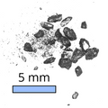
Indium(II) Selenide Powder
Can be used in electronic and optical devices and in the preparation of InSe nanosheets or nanoparticles by liquid chemical exfoliation or chemical vapor deposition
Available in quantities of 500 mg or 1 g
≥99.995% purity
From £220
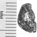
Indium(II) Selenide Crystals by Size
Can be used as a semiconductor, in non-linear optics, and to produce 2D monolayer and few-layer InSe by mechanical or liquid exfoliation
Small (≥10 mm2) or medium (≥25 mm2) available*
≥99.999% purity
From £520
*Typical representative size, areas/dimensions may vary.
Technical Data
| CAS Number | 1312-42-1 |
| Chemical Formula | InSe |
| Molecular Weight | 193.78 g/mol |
| Bandgap | 1.3 - 2.0 eV |
| Preparation | Synthetic, by chemical vapor transport (CVT) |
| Structure | Rhombohedral |
| Electronic Properties | 2D semiconductor |
| Melting Point | 600 °C (lit.) |
| Color | Dark brown |
| Synonyms | Indium monoselenide |
| Classification / Family | Transition metal dichalcogenides (TMMCs), 2D semiconductor materials, Nano-electronics, Nano-photonics, Photovoltaic, Materials science |
Product Details
| Form | Purity |
|---|---|
| Powder | ≥99.995% |
| Crystal | ≥99.999% |
Pricing Table
| Product Code | Form | Size/Weight* | Price |
|---|---|---|---|
| M2135C1 | Powder | 500 mg | £220 |
| M2135C1 | Powder | 1 g | £350 |
| M2135A10 | Crystal | Small (≥10 mm2) | £520 ea. |
| M2135A25 | Crystal | Medium (≥25 mm2) | £850 ea. |
*typical representative size, areas/dimensions may vary.
MSDS Documents
Structure of Indium(II) Selenide
Single layer of indium(II) selenide (InSe) consists of four mono-atomic sheets of hexagonally arranged atoms tetrahedrally linked in the sequence of Se–In–In–Se via covalent bonds. Each of the two indium atoms is bound to three neighbouring selenides. At room temperature under ambient conditions, InSe crystallizes in a rhombohedral layered phase, known as γ-InSe with a space group of R3m.
Each of its layers has a honeycomb lattice made of indium and selenium atoms. The layers are bound by relatively weak van der Waals forces which allow mechanical or wet exfoliation to obtain atomically thin films.

Literature and Reviews
Indium(II) Selenide Powder in Literature
- The direct-to-indirect band gap crossover in two-dimensional van der Waals Indium Selenide crystals,G. W. Mudd et al., Sci. Rep., 6:39619 (2016); DOI: 10.1038/srep39619.
- High Performance and Bendable Few-Layered InSe Photodetectors with Broad Spectral Response, S. Tamalampudi et al., Nano Lett. 2014, 14, 2800−2806 (2014); doi: 10.1021/nl500817g.
- Structural modification and band-gap crossover in indium selenide nanosheets, M. Airo et al., RSC Adv., 6, 40777 (2016); DOI: 10.1039/c6ra00262e.
Indium(II) Selenide Crystals in Literature
- The direct-to-indirect band gap crossover in two-dimensional van der Waals Indium Selenide crystals, G. W. Mudd et al., Sci. Rep., 6:39619 (2016); DOI: 10.1038/srep39619.
- High Performance and Bendable Few-Layered InSe Photodetectors with Broad Spectral Response, S. Tamalampudi et al., Nano Lett. 2014, 14, 2800−2806 (2014); doi: 10.1021/nl500817g.
- Structural modification and band-gap crossover in indium selenide nanosheets, M. Airo et al., RSC Adv., 6, 40777 (2016); DOI: 10.1039/c6ra00262e.
Related Products
We stock a wide range of 2D materials available to purchase online. Please contact us if you cannot find what you are looking for.