Titanium(IV) Selenide (TiSe2) Powder and Crystal
CAS Number 12067-45-7
Transition Metal Dichalcogenides (TMDs), Transition Metal Chalcogenides (TMCs), 2D Materials, Low Dimensional Materials,Low price, high purity 2D metal titanium(IV) selenide powder and crystals
For the development of next-generation electronics, optoelectronics, and nanotechnology
Technical Data | MSDS | Structure | Literature and Reviews | Related Products | Resources and Support
Titanium(IV) selenide (also known as titanium diselenideTiSe2), CAS number 12067-45-7, is a family member of Group IV transition metal dichalcogenides (TMDCs), and is of great interest as one of the typical charge density wave (CDW) materials. It is known that the CDW characteristics of TiSe2 can be changed; they are typically suppressed. In some cases, this leads to superconductivity or magnetic order by applying high pressure or intercalation.
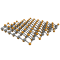
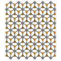
TiSe2 has an octahedral crystal structure (1T, space group D3d) with van der Waals stacked layers. In its bulk form, 1T-TiSe2 undergoes a phase transition from a semimetal (1 × 1 × 1 normal phase) to a commensurate CDW (2 × 2 × 2 CDW) at around 200 K. Recent discoveries have demonstrated that superconductivity in TiSe2 can be induced either by field-effect doping of few-layer TiSe2, or copper doping to form CuxTiSe2. In both cases, the suppression of the CDW is considered essential to achieve superconductivity.
TiSe2 has an electronic structure near the Fermi energy level comparable to that of a semiconductor. Its valence and conduction bands overlap slightly through an indirect gap. Rather interestingly, TiSe2 has an exotic ground state, the 'excitonic insulator' phase.
High Purity
≥99.999% Crystal Purity
Worldwide shipping
Quick and reliable shipping
Low Cost
Low Cost Titanium(IV) Selenide
Powder & Crystal
Different Forms of Titanium(IV) Selenide
We supply low price titanium(IV) selenide in several different forms for a range of applications.
Titanium(IV) Selenide Powder
Can be used for preparation of titanium(IV) selenide nanoplates and ultrathin films
Sold by weight
≥99.995% purity
From £350
Titanium(IV) Selenide Crystals by Size
Can be used to produce single or few-layer titanium(IV) selenide sheets via mechanical or liquid exfoliation
Small (≥10 mm2) or medium (≥25 mm2) crystals available*
≥99.999% purity
From £520
*Typical representative size, areas/dimensions may vary
Bulk single titanium(IV) selenide crystal is most commonly used as sources from which single or few-layer sheets can be obtained via either mechanical or liquid exfoliation.
Titanium(IV) selenide powder can also be used to prepare TiSe2 nanosheets and nanoparticles by liquid-exfoliation (normally assisted by sonication).
Technical Data
| CAS Number | 12067-45-7 |
| Chemical Formula | TiSe2 |
| Molecular Weight | 205.79 g/mol |
| Bandgap | N/A |
| Preparation | Synthetic - Chemical Vapor Transport (CVT) |
| Structure | Octahedral (1T) |
| Electronic Properties | Semimetal, Charge Density Waves (CDW) |
| Melting Point | N/A |
| Color | Dark brown |
| Synonyms | Titanium Diselenide (TiSe2), Bis(selanylidene)titanium |
| Classification / Family | Transition metal dichalcogenides (TMDCs), Charge Density Wave (CDW), Superconductivity, Nano-electronics, Nano-photonics, Photovoltaic, Materials science |
Product Details
| Form | Purity |
|---|---|
| Powder | ≥99.995% |
| Crystal | ≥99.999% |
Pricing Table
| Product Code | Form | Size/Weight* | Price |
|---|---|---|---|
| M2151C1 | Powder | 1 g | £350 |
| M2151A10 | Crystal | Small (≥10 mm2) | £520 ea. |
*Typical representative size, areas/dimensions may vary
Shipping is free for qualifying orders.
MSDS Documents
Structure of Titanium(IV) Selenide
TiSe2 has an octahedral crystal structure (1T, space group D3d) with van der Waals stacked layers. Monolayer TiSe2 consists of stacked Se–Ti–Se atomic layers, in which Ti and Se atoms are strongly bound within the layer. Ti atom is located in the center of the octahedral, which is the inversion symmetry point.

Literature and Reviews
- Enhancing charge-density-wave order in 1T-TiSe2 nanosheet by encapsulation with hexagonal boron nitride, L. Li et al., Appl. Phys. Lett. 109, 141902 (2016); doi: 10.1063/1.4963885.
- Unveiling the charge density wave inhomogeneity and pseudogap state in 1T-TiSe2, K. Zhang et al., Sci. Bull., 63, 426–432 (2018); doi: 10.1016/j.scib.2018.02.018.
- Unconventional Charge-Density-Wave Transition in Monolayer 1T‑TiSe2, K. Sugawara et al., ACS Nano, 10, 1341−1345 (2016); DOI: 10.1021/acsnano.5b06727.
Related Products
We stock a wide range of 2D materials available to purchase online. Please contact us if you cannot find what you are looking for.