OFET Device Testing & Fabrication Equipment

Ossila's OFET Equipment provide several options for fabrication and testing of OFET devices. We have created an eco-system of substrates, testing systems and deposition aids to make OFET research as straight forward as possible.
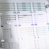
Most of our OFET equipment is designed around two architectures: high density and low density.By using these device designs, you can reliable and consistently change variable, and test devices quickly and easily test using our OFET test boards:
- The low density OFET design are designed with relatively large channels so contact effects are minimized. This means that matching energy levels matching of the active layer and the source-drain contacts is less important. Also, the 30 mm channel length produces larger currents for quicker measurements that can be measured with less sensitive equipment.
- High density OFETs allow you to test up to 20 OFETs on a single substrate. This makes testing OFET devices quicker with better statistical results.

Jump to: Browse OFET Equipment | Using Evaporation Masks | Resources and Support
Browse Products
Filter by OFET Density:
Filter by Application:


Using OFET Masks
The Ossila OFET Masks are designed to be used with vacuum based deposition technique such as thermal evaporation. In thermal evaporations, OFET layers are heated in vacuum conditions until they vaporize. The vaporized materials travel upwards then condense onto a substrate, forming uniform layers. Thermal evaporation is widely used because it produces high-purity films and enables the fabrication of multilayer OFET structures with well-defined interfaces.
Resources and Support
 Organic Field Effect Transistors (OFET)
An organic field effect transistor (OFET) is a device that uses a small gate voltage to control the current flow across an organic semiconductor material. This type of organic thin film transistor (OTFT) serves as an alternative to silicon-based field effect transistors such as MOSFETs. OFET devices consist of drain and source electrodes, a dielectric layer, an organic semiconductor (OSC) and a voltage electrode.
Read more...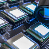 OTFT & OFET Fabrication Guide
This guide describes how to fabricate OFETs using Ossila substrates, equipment and masks. These interconnected items allow you to rapidly screen organic layers using solution processing or evaporation methods. On this page, we tested achieved mobilities approaching 10-2 cm2/Vs via solution processing methods, based on the organic semiconductor P3HT with a PMMA gate insulator and a PEDOT:PSS gate electrode.
Read more... Long Channel OFET Fabrication System Overview
The Long Channel Organic Field-Effect Transistor (OFET) source/drain evaporation stack is designed to make fabrication as simple as possible so you can focus on material testing rather than fabrication.
Read more...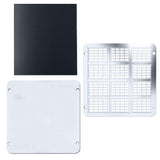 How to Load the High Density OFET Stack
Fluorescence and phosphorescence are types of photoluminescence. Photoluminescence refers to radiative emissions where the absorbance of a photon is followed by the emission of a lower energy photon.
Read more...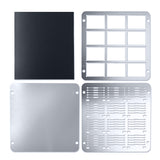 How to Load the Low Density OFET Stack
How to load the low density OFET stack - Carefully place the evaporation mask on the lower support of the evaporation stack. Place the upper support / substrate holder on top of the evaporation mask
Read more... What are Organic Electrochemical Transistors (OECTs)?
Organic electrochemical transistors (OECTs) regulate charge flow through an organic semiconductor channel via ion injection from an electrolyte. The most common organic semiconductor used is PEDOT:PSS. In OECTs, ionic and electronic charges can couple throughout the entire volume of the channel, resulting in higher transconductance compared to Field-Effect Transistors (FETs). However, due to ion diffusion, OECTs have slower response times.
Read more...