FREE shipping on qualifying orders when you spend or more. All prices ex. VAT. Enjoy hassle-free delivery, fulfilled by our EU subsidiary. Backed by our 50 State Delivery Guarantee. Regional distributors also available. Sorry, we are unable to accept orders from or ship to .

It looks like you are using an unsupported browser. You can still place orders by emailing us on info@ossila.com, but you may experience issues browsing our website. Please consider upgrading to a modern browser for better security and an improved browsing experience.

Evaporation Stack for OFETs, Low Density

Substrates and Fabrication

Product Code E281
Price $429 ex. VAT

Low Density Evaporation Stack for OFETs

Enabling accurate deposition resolution


Overview | Specifications | Resources


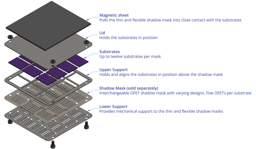
The evaporation stack holds the OFET source-drain shadow masks (sold separately) and substrates in close contact for thermal evaporation. This is crucial for effective device fabrication as the source-drain channel is usually the most critical feature on an OFET. For use with the Ossila low density OFET source-drain evaporation masks and Silicon Oxide Substrates.

Specifications


Size 75 mm x 75 mm
Thickness 1 mm (exc. bolts)
Material Stainless steel
Capacity 12 substrates

System Overview


The low density fabrication system has four different masks available (source-drain, gate deposition, active area deposition and insulator deposition) to allow the fabrication of devices in any geometry (top/bottom gates and top/bottom source-drain). The diagrams below show the features on each of the individual masks as well as how they fit together on a substrate.

OFET evaporation stack low density
Schematic diagram showing how the different evaporation masks fit together on a device. For back-gate Si/SiO2 substrates, the insulator and gate masks are not required as the gate contacts on the source-drain mask wrap around to contact the central Si layer of the substrate.
 Ossila low density evaporation masks
The layer order for an FET using the low density evaporation masks.


Ossila back-gated FET using Si/SO2 substrates
The layer order for a back-gated FET using Si/SO2 substrates.

Note that silicon oxide substrates do not need a gate mask which simplifies fabrication, however the use of a gate mask with quartz-glass substrates can allow lower operating voltages and lower parasitic capacitance.

Resources and Support


How to load the Low density OFET stack

This video demonstrates how to load the Low density OFET stack typically used to thermally evaporate (vacuum deposit) source-drain contacts. The video shows how to carefully place the evaporation mask on the lower support of the evaporation stack.

Learn more...
Return to the top