Substrates and Fabrication

Quickly and easily fabricate and characterize thin-film devices for OPVs, OLEDs, OFETs/TFTs and sensors with our range of substrates and fabrication accessories. We have also designed a number of test chips and boards to take the hassle out of device testing; our electronic test boards have a simple push-fit design with connection pins that align perfectly with the contacts on our substrates.
If you're looking to fabricate photovoltaics or OLEDs, the latest 8-pixel design of substrates and masks allow you to create either eight small individual pixels or a single large pixel.
Jump to: Browse all products | Compatible products | Resources and support
Browse Substrates and Fabrication Supplies
Related categories: all lab equipment, electrical test boards, solution making supplies, general laboratory supplies
Filter by product:
Filter by system:


Looking for generation I or generation II systems? We have discontinued our generation I and generation II substrates and masks. Contact us for more information or for help migrating to the new 8-pixel design.
Choosing the Right System
Find out which products are compatible. The tables below use product codes; if you are not sure which components you have, you can find each product by searching the product code on our website.
Jump to: Patterned ITO | Unpatterned ITO | Quartz | ITO OFET | Patterned FTO | Unpatterned FTO | Low Density FET | High Density FET
Patterned ITO
| Substrate | Evaporation Mask | Aperture Mask | Riser Board | Test Board |
|---|---|---|---|---|
| S211 | E501 | E521 | P2009B2 | P2008A1 |
| E502 | E522 | |||
| E503 | E521 | |||
| E504 | – | |||
| E531 | E521 | |||
| E632 | – | |||
| S241 | E601 | – | P2009F2 | P2012A1 |
| E602 | – | |||
| S251 | E611 | – | P2009F2 | P2012A1 |
| S2006C1 | E2001A1 | E2002A1 | P2009E2 | P2011A1 |
| E2001B1 | E2002A1 | |||
| E2003A1 | E2002B1 | |||
| E2003B1 | E2002B1 | |||
| E2004A1 | E2002A1, E2002B1 |
Unpatterned ITO
| Substrate | Evaporation Mask | Aperture Mask | Riser Board | Test Board |
|---|---|---|---|---|
| S111 | E501 | E521 | P2009B2, P2009G2 | P2008A1, P2008B1 |
| E502 | E522 | |||
| E503 | E521 | |||
| E504 | – | |||
| E531 | E521 | |||
| E632 | – | |||
| S281 | E601 | – | P2009F2, P2009G2 | P2012A1 |
| E602 | – | |||
| E611 | – | |||
| S2006B1 | E2001A1 | E2002A1 | P2009E2, P2009G2 | P2008A1, P2011A1 |
| E2001B1 | E2002A1 | |||
| E2003A1 | E2002B1 | |||
| E2003B1 | E2002B1 | |||
| E2004A1 | E2002A1, E2002B1 |
Quartz
| Substrate | Evaporation Mask | Aperture Mask | Riser Board | Test Board |
|---|---|---|---|---|
| S151 | E501 | E521 | P2009B2, P2009G2 | P2008A1, P2008B1 |
| E502 | E522 | |||
| E503 | E521 | |||
| E504 | – | |||
| E531 | E521 | |||
| E632 | – | |||
| S261 | – | – | P2009G2 | – |
| S2006A1 | E2001A1 | E2002A1 | P2009E2, P2009G2 | P2008A1, P2011A1 |
| E2001B1 | E2002A1 | |||
| E2003A1 | E2002B1 | |||
| E2003B1 | E2002B1 | |||
| E2004A1 | E2002A1, E2002B1 |
ITO OFET
| Substrate | Evaporation Mask | Aperture Mask | Riser Board | Test Board |
|---|---|---|---|---|
| S161 | E271, E309 | – | – | P2013A1 |
| S162 | E271, E309 | – | – | P2013A1 |
Patterned FTO
| Substrate | Evaporation Mask | Aperture Mask | Riser Board | Test Board |
|---|---|---|---|---|
| S212 | E501 | E521 | P2009B2 | P2008A1 |
| E502 | E522 | |||
| E503 | E521 | |||
| E504 | – | |||
| E531 | E521 | |||
| E632 | – | |||
| S2008C1 | E2001A1 | E2002A1 | P2009E2 | P2011A1 |
| E2001B1 | E2002A1 | |||
| E2003A1 | E2002B1 | |||
| E2003B1 | E2002B1 | |||
| E2004A1 | E2002A1, E2002B1 |
Unpatterned FTO
| Substrate | Evaporation Mask | Aperture Mask | Riser Board | Test Board |
|---|---|---|---|---|
| S301, S303, S304, S2009B1 |
E501 | E521 | P2009B2, P2009G2 | P2008A1, P2008B1 |
| E502 | E522 | |||
| E503 | E521 | |||
| E504 | – | |||
| E531 | E521 | |||
| E632 | – | |||
| S2004S1, S2003S1, S2001S1, S2002S1 |
E2001A1 | E2002A1 | P2009E2, P2009G2 | P2008A1, P2011A1 |
| E2001B1 | E2002A1 | |||
| E2003A1 | E2002B1 | |||
| E2003B1 | E2002B1 | |||
| E2004A1 | E2002A1, E2002B1 |
Low Density FET
| Substrate | Evaporation Mask | Aperture Mask | Riser Board | Test Board |
|---|---|---|---|---|
| S146, S148 | E281 | – | – | P2013A1 |
| E291 | – | – | ||
| E292 | – | – | ||
| E307 | – | – | ||
| E309 | – | – | ||
| E305 | – | – | ||
High Density FET
| Substrate | Evaporation Mask | Aperture Mask | Riser Board | Test Board |
|---|---|---|---|---|
| S146, S148 | E312 | – | – | P2013A1, P2014A1 |
| E321 | – | – | ||
| E322 | – | – | ||
| E323 | – | – | ||
| E338 | – | – | ||
| E3310 | – | – | ||
| E336 | – | – | ||
| E337 | – | – | ||
| S403A1, S403A2 | E312 | – | – | P2014A1 |
| E338 | – | – |

Resources and Support
 How to Load the Low Density OFET Stack
Carefully place the evaporation mask on the lower support of the evaporation stack. Place the upper support / substrate holder on top of the evaporation mask.
Read more... How to Load the High Density OFET Stack
Carefully place the evaporation masks into the substrate holder. Place the silicon substrates on top of the masks with the polished surface touching the mask
Read more... What are Transparent Conductive Oxides?
Transparent conductive oxides (TCOs) are metal oxides, such as zinc oxide and tin oxide, that are capable of conducting electricity whilst being optically transparent. This means they absorb a low number of electromagnetic waves within the visible region of the spectrum, appearing see-through.
Learn more... Organic & Thin Film Field Effect Transistor Fabrication Guide
The Ossila pre-patterned OFET substrates have been designed to enable the fabrication and characterization of transistors without the need for vacuum evaporation systems or probe stations.
Read more... Long Channel OFET Fabrication System Overview
The Long Channel Organic Field-Effect Transistor (OFET) source/drain evaporation stack is designed to make fabrication as simple as possible so you can focus on material testing rather than fabrication.
Read more...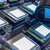 OLED Fabrication Guide
In this guide, we demonstrate how to make standard organic light-emitting diode devices in a glove box using materials and equipment easily available to any lab. Find out more.
Read more...