OTFT & OFET Fabrication Guide
Jump to: Choosing Substrates | Device Architectures | Solution Processed OFETs | OFET Evaporation | OFET Measurement | Equipment List | Acronyms
This guide describes how to fabricate and test organic thin film transistors (OTFTs and organic field effect transistors (OFETs) using Ossila substrates, equipment and masks. These interconnected items allow you to rapidly screen organic layers using either solution processing or evaporation methods. On this page, we tested achieved mobilities approaching 10-2 cm2/Vs via solution processing methods, based on the organic semiconductor P3HT with a PMMA gate insulator and a PEDOT:PSS gate electrode.
Ossila OFET substrates and testing boards have been designed to facilitate the fabrication and characterization of transistors using solution processing methods. Most OFET configurations require probe stations to fully characterize their performances. Full characterization stations, such as the electrical characterization system, are ideal if you need to conduct various types of electrical measurements on various device architectures.
However, devices fabricated using Ossila Prefabricated OFET test chips, or the OFET ITO substrates can also be tested using the compatible OFET testing boards. These devices can be produced quickly and easily, making them ideal for high throughput material screening experiments as well as teaching and training purposes.
OFET Testing & Fabrication Equipment

Video Guide
Watch the accompanying fabrication video to see the process in action.
Choosing Substrates
The pre-patterned OFET substrates have interdigitated ITO fingers which act as the source-drain contacts with overall channel dimensions of 30 mm x 50 µm. These relatively large channels mean that contact effects are minimized, so matching the energy levels of the organic semiconductor and contacts is less important. The intrinsic Poole–Frenkel (bulk) limited mobility of a material can be more easily assessed independent of contact effects. The 30 mm channel length also has the additional benefit of producing larger currents, making testing and measurement quicker and requiring less sensitive (less expensive) equipment.

Alternatively, you can also use unpatterned quartz glass substrates and build the device you want from scratch. Deposit each layers using our evaporation masks or to your own design to suit your architecture. Our quartz substrates are made of high-quality soda-lime float glass with a 20 nm coating of SiO2 (synthetic quartz). These substrate are ultra-flat, inert and robust allowing tough pre-coating treatments such as OFT and HMDS to improve mobility. The transparent nature of the ITO-glass /quartz-glass means these substrates are also perfect for conducting opto-electric experiments.
Ossila also offer Platinum Test Chips for the fastest and easiest OFET material screening. These chips consist of Si/SiO2 layers which act as the gate contact layer, and dielectric layer. These have a back-contact, back-gate architecture where all layers but the organic semiconductors have been deposited. Therefore, you simply solution process an organic layer on these chips and test using the High Density OFET testing board.
Device Architecture
Most OFET and OTFT devices require a probe system for accurate testing. This allows you to test a range of different device types, and doesn't lock you in to one particular architecture. In other words, using a probe station give you the most flexibility with OFET testing.
However, Ossila have also created an eco-system of compatible substrates and testing boards to negate the need for a probe station. For example, you can easily create an OFET device by depositing an organic semiconductor, gate insulator and gate on the OFET ITO substrates. The ITO is patterned on this substrate with ready made source and drain pins, as well as a bus bar for gate electrode connection. By using a solution based synthetic metal such as PEDOT:PSS for the gate electrode, you can make fully-functioning OFETs by solution processing alone - thus eliminating the need for vacuum evaporation processes. With the Ossila OFET test board, you can test these devices with just the flick of a switch.

In the fabrication example described above, the materials are all processed from solution with P3HT used as the organic semiconductor, PMMA as the gate insulator and PEDOT:PSS as the gate. Transistors are fabricated in a matter of minutes once solutions have been prepared and the substrates have been cleaned. However, these substrates also compatible with other material systems and deposition techniques.
The below diagram shows an example OFET device architecture (specifically the Ossila Low Density OFET architecture) using 4 evaporation masks (source-drain, gate deposition, active area deposition and insulator deposition). By changing the order the layers are deposited, you can change the type of device. However, different architectures require different substrates.
In the left image below, starting with a quartz transparent substrate, you deposit the source/drain electrodes, then the active area, then the insulator or dielectric material, then the gate. This creates a devices with a back-contact top-gate architecture. However if using a Si/SiO2 substrate, you can just deposit the source/drain electrodes, then the active layer to create a BGBC architecture.


Solution Processed OFETs
One of the benefits of using organics in electronic devices is that they can be solution processed via methods like spin coating and slot die coating. Below describes an example for how to create a solution processed OFET device.
Cleaning
To create a high-performance device, you always need a pristine, clean surface. Therefore, your cleaning processes are very important.
When making OFET devices, you can clean your substrates using the classic substrate cleaning method. An alternative technique involves cleaning substrates with a combination of a high performance electronic-grade cleaning agent and immersion in sodium hydroxide (NaOH). The NaOH treatment modifies the surface by addition of OH- groups and provide a hydrophilic interface without the need for plasma cleaning. For a high-performance electro-optical cleaning agent, we recommend using Hellmanex III as this provides excellent cleaning performance without leaving a residue on the surface. For the sodium hydroxide solution we typically make a stock solution of 10% by weight in water. To make cleaning faster and easier, we generally clean substrates in batches using a substrate rack. The use of a substrate rack also has the additional benefits of preventing substrates from scratching each other and enhances cleaning by keeping them vertical so that particulates naturally fall off. Make sure to handle the devices with tweezers at all times to avoid contamination.
You can also use supplementary surface treatment techniques, such as plasma cleaning or a UV-ozone cleaner, to further prepare the substrate for wetting.
When loading a substrate rack, arrange the substrates so that they all have the same orientation as it is easier to identify the top (ITO) side at this stage. To identify the ITO side, simply look at the edge of the substrate at an oblique angle; the ITO should be seen to go all the way to the edge when facing towards the viewer. This is most obvious when reflecting a light source and so getting the correct positioning of light, substrate and eye makes this task much quicker.


An example cleaning routine is as follows:
- Sonicate in hot 10% NaOH for 5 minutes.
- Dump rinses (hot water, hot water)
- Sonicate in hot 2% Hellmanex for 5 minutes.
- Dump rinses (hot water, hot water, cold DI water)
- Sonicate in IPA (cold) for 5 minutes
- Blow dry using dry nitrogen
Note: Always take additional care when handling acid/bases especially when hot and always file appropriate risk assessments with your departmental safety officer before undertaking work. Also note that after both the Hellmanex and NaOH treatments, the substrates are "dump rinsed" to remove the cleaning agent. This consists of placing them in three successive beakers of water, the first two of which contain boiling water and the third one de-ionized (DI) water.
Spin Coating
OFETs were fabricated in a bottom-contact top-gate configuration with the following layers spun sequentially.
- Surface treatment (HMDS)
- Organic semiconductor (P3HT)
- Gate insulator (PMMA)
- Gate electrode (PEDOT:PSS)
Surface Treatments
Surface treatments are important to obtain high mobilities from P3HT OFETs. Therefore, a spin-coated HMDS surface treatment was used prior to P3HT deposition. However, vapor phase HMDS or liquid phase OTS treatments will also work.
Active Layer
In the example devices shown here, P3HT is used as the organic semiconductor. However, other polymeric semiconductors can be used such as PCDTBT or PBTTT. In order to maximize the performance, we dissolved a medium molecular weight P3HT (Ossila M107, Mw = 24,480 kDa) in a high boiling-point solvent 1,2,4-Trichlorobenzene (TCB) at a concentration of 10 mg/ml. This solution was dissolved on a hotplate at 80°C for 30 minutes with stirbar (1000 rpm). After this, it was left to cool to room temperature over 10 minutes and filtered with a 0.45 μm PTFE (hydrophobic) membrane filter.
Gate Insulator
As this methods uses sequential spin coating, the choice of gate dielectric and its corresponding solvent are also critical. An orthogonal solvent system is required to ensure that the active semiconductor is not washed away when the gate dielectric is deposited.
For most polymeric semiconductors, PMMA dissolved in butan-2-one can be used as the gate dielectric. The molecular weight of the PMMA is important because a thick uniform film is required. Here, we used PMMA with a molecular weight of 120,000 and dissolve it at 100 mg/ml in butan-2-one. The subsequent film provides the thickest possible films to reduce gate leakage. Molecular weights significantly higher than this will cause solubility issues and uneven films while significantly. Molecular weights lower than this can cause pin-holes and solvent incompatibility with solution processed gate electrodes. To aid dissolution, the solution was heated for 30 minutes at 80°C and stirred at 1000 rpm before being left to cool to room temperature over 10 minutes and filtered through a 0.45 µm PTFE (hydrophobic) membrane filter.
Processing Conditions
All stages of the organic deposition were performed within a nitrogen glove box. However, when used with suitably stable semiconductors (such as PCDTBT), these steps could also be performed in air.
Different spin coating techniques are used for the various layers. The HMDS layer is statically dispensed, where the substrate is first covered in solution and then spin coating process started. The P3HT and the PMMA layer are dynamically spin coated, while the substrate is already spinning. A static dispense can often give better coverage at spin speeds below 1000 rpm and also give more time for surface interactions which is why this technique was used for the HMDS. Meanwhile a dynamic dispense is often preferable at high spin speeds and for fast-evaporating solvents and uses much less material (at 1000 rpm and above 20 µl is usually sufficient).
When spun from TCB, the P3HT requires two-stage spin due to its high boiling point, and consequently, slow drying time. Typically the first stage defines the desired thickness over the majority of the substrate and a second, much faster, stage is used to drive leftover solvent evaporation.
The spin coating regime for the transistors can therefore be summarized below. If you are using a programmable spin-coater, such as the Ossila Spin Coater, all three layers can be applied consecutively without the substrate ever being allowed to stop. This allows for faster fabrication and can also be used to minimize the exposure of the organic semiconductor to air if being spun under ambient conditions.
| Step | Spin Speed | Duration | Comments |
|---|---|---|---|
| HMDS | 2000 rpm | 30 s | 100 µl static deposition |
| P3HT - Stage 1 | 1500 rpm | 150 s | 30 µl dynamic deposition |
| P3HT - Stage 2 | 4000 rpm | 30 s | No deposition - just drying |
| PMAA | 1000 rpm | 30 s | 100 µl dynamic deposition |
Patterning and Annealing
- After depositing the P3HT layer, wipe clean from the edges and the contact pads with a cleanroom swab dipped in chlorobenzene.
- After depositing, you can scratch off the PMMA layer from the gate and contact pads using precision tweezers.
- Once all layers are deposited, anneal at 105 °C for five minutes.
Gate Electrode
After the PMMA layer, you should deposit a gate electrode. A solution-processed gate enables rapid fabrication without the use of costly and slow vacuum deposition equipment. However, any solution-processed gate also needs to be solvent compatible with the gate insulator (and preferably organic semiconductor as well). It should also have the right wetting and film-forming properties to enable uniform substrate coverage.
A high conductivity PEDOT:PSS formulation such as PH 1000 PEDOT:PSS can be applied on top of the PMMA if mixed with additives to control the wetting properties. We have found that the following recipe works well for our devices:
NMP is a solvent for increasing conductivity to PH1000. Triton X-100 is a surfactant to ensure complete mixing. IPA is used to improve spin coating by improving the repeatability, wettability and drying.
| Component | Order to add | % by weight |
| PH1000 PEDOT:PSS | 1 | 42.5 |
| N-Methyl-2-pyrrolidone (NMP) | 2 | 2.5 |
| Triton X-100 | 3 | 1 |
| Isopropyl Alcohol | 4 | 54 |
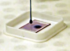
Spin coat PEDOT:PSS mixture
- Spin coat using a 50 µl dynamic dispense at 4000 RPM
- Wipe clean the contact pads using cleanroom swab dipped in IPA
It is important that this solution should make contact with the gate electrode strip, but not the source-drain contacts (see schematic below).
Alternatively, a few drops of the PEDOT:PSS mixture can simply be placed over the electrode areas and left to dry slowly under atmospheric conditions. However this is less repeatable than spin coating the substrates.
OFETs Via Evaporation Techniques
The most commonly used deposition methods for FET devices are techniques like thermal evaporation, e-beam deposition or sputter coating. These techniques allow for extremely controlled deposition of high purity, uniform layers. Also, by using deposition mask, you can carefully control patterning of each layer to optimize device architecture.
To deposit layers, you will need to place your substrates in an holder with an appropriate mask. An example of this process is shown in the video below.
In thermal evaporation, thin films are deposited under high vacuum. Metal electrodes and organic semiconductors are heated in separate sources until they vaporize. The vaporized materials travel upwards then condense onto a substrate, forming uniform layers. Thermal evaporation is widely used because it produces high-purity films and enables the fabrication of multilayer OFET structures with well-defined interfaces.
OFET Measurement
Measurement of OFET or OTFT devices requires three terminals connected through two interacting circuits. A voltage bias is applied between the source and drain electrodes to drive current, while an independent gate bias controls the channel conductance. OFET performance can be determined by measuring the output curve (Isource-drain against Vsource-drain) at various gate voltages, and the transfer curve (Isource-drain against Vgate).
In most cases, this process is controlled using several micromanipulators within a probe station. For OFET and OTFT devices, you will likely need drain voltages exceeding 10 V, so other source measure units may be needed.
The devices in this article were characterized using a dual source-measure unit under computer control. An Ossila Low Density OFET Test board was used to connect and switch between the individual OFETs on a substrate. In this case, testing was performed under ambient atmosphere in darkness. However, the OFET measurement board is designed to be small enough to fit inside a glove box to enable measurements under an inert atmosphere as well. When testing under ambient conditions, exposure to air and light levels must be minimized. As such, we recommend storing the finished devices in sealed vials until measurement.
For the output characteristics the drain voltage was swept from +12 V to -40 V for each gate voltage tested from +10 V to -40 V (in -10 V steps); for the transfer characteristics the gate voltage was swept from +12 V to -40 V for each of the two drain voltages tested (-4 V and -40 V). It is recommended that three of each characteristic test is run, to enable the device to “burn-in”.
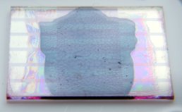
The data obtained from the device pictured above can be seen below, the device shows good saturation in the output characteristics, while the transfer plot reveals a mobility of 9.26 x 10⁻³ cm2V-1s-1 and a threshold voltage -2.31 V. This compares with the highest reported values in the literature for P3HT in the region of 10-1 cm2V-1s-1 from devices with vacuum-deposited gold electrodes and typical channel lengths of <25 µm.


Equipment List
Processing Equipment
- Spin Coater
- 2 hot-plates (one held at 70°C for solutions and one held at 90°C for substrates)
- Polypropylene cleaning beaker
- Substrate rack
- Ultra-sonic bath
- Variable volume micropipette
Consumables Needed
- Hellmanex III
- Pre-patterned ITO OFET substrates
- PEDOT:PSS (PH1000 PEDOT:PSS)
- 0.45 µm PES and 0.45 μm PTFE (hydrophobic) filters
- Solvent resistant syringes
- Micro-precision cleaning swab
- Isopropyl alcohol
- Encapsulation epoxy
- Glass coverslips
- Micropipette Tips
OFET Device Testing & Fabrication Equipment

Acronyms and Molecular Structures
| HMDS | Hexamethyldisilazane |
| HOMO | Highest occupied molecular orbital |
| IPA | Isopropyl alcohol |
| ITO | Indium tin oxide |
| NaOH | Sodium hydroxide |
| NMP | N-Methyl-2-pyrrolidone |
| OFET | Organic field effect transistor |
| OTS | Octadecyltrichlorosilane |
| P3HT | Poly(3-hexylthiophene-2,5-diyl) |
| PBTTT | Poly(2,5-bis(3-tetradecylthiophen-2-yl)thieno[3,2-b]thiophene) |
| PCDTBT | Poly[N-9'-heptadecanyl-2,7-carbazole-alt-5,5-(4',7'-di-2-thienyl-2',1',3'-benzothiadiazole)] |
| PEDOT:PSS | Poly(3,4-ethylenedioxythiophene) poly(styrenesulfonate) |
| PES | Polyether sulfone |
| PMMA | Poly(methyl methacrylate) |
| PTFE | Polytetrafluoroethylene |
| RPM | Revolutions per minute |
| TCB | 1,2,4-Trichlorobenzene |
PEDOT Polymer Blends

Learn More
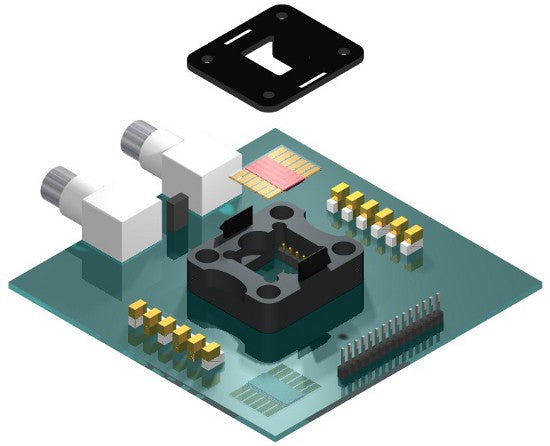
 Long Channel OFET Fabrication System Overview
The Long Channel Organic Field-Effect Transistor (OFET) source/drain evaporation stack is designed to make fabrication as simple as possible so you can focus on material testing rather than fabrication.
Read more... What are Organic Electrochemical Transistors (OECTS)?
Organic electrochemical transistors (OECTs) regulate charge flow through an organic semiconductor channel via ion injection from an electrolyte. The most common organic semiconductor used is PEDOT:PSS.
Read more...