
Low Density OFET Test Board
Designed with maximum experimental versatility in mind
Perfect for high-precision, low-current measurement.
The Ossila Low Density OFET Test Board is designed to work with our pre-patterned substrates, eliminating the need for probe stations - making electrical contact to devices quick and simple.
Datasheet
The Ossila Low Density OFET Test Board is ideal for high-precision, low-current measurement. When switched off, the transistor current can be as low as a few hundred pico Amperes. Normally, a high accuracy of current is difficult to achieve in the nano-ampere range or lower, as it is difficult to isolate the test components (BNC cables, switches, board). Furthermore, with electromagnetic noise, stray capacitance current can introduce non-negligible error. We've worked to reduce this with the following features:
- Double ground plane - helps to isolate the board from external noise
- Intelligent design of the board's wire tracks - reduces noise, leakage current, stray capacitance
- Switch selection - Improved switches show almost no extra resistance to current flow when ON, and more importantly, do not introduce leakages current when OFF
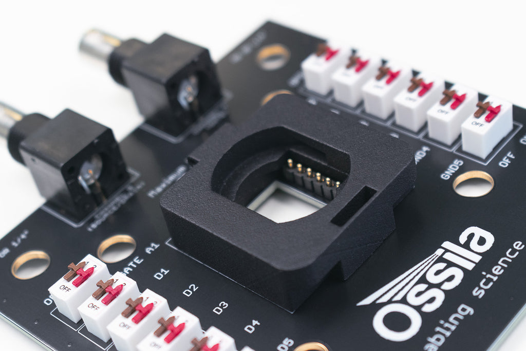
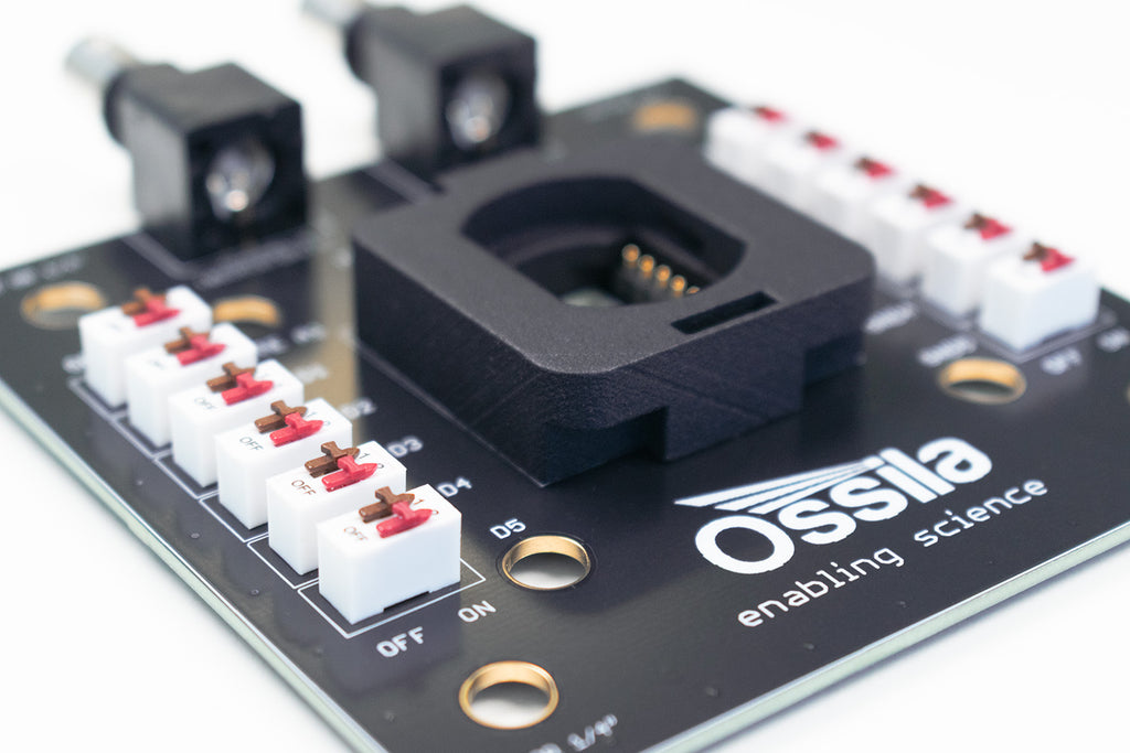
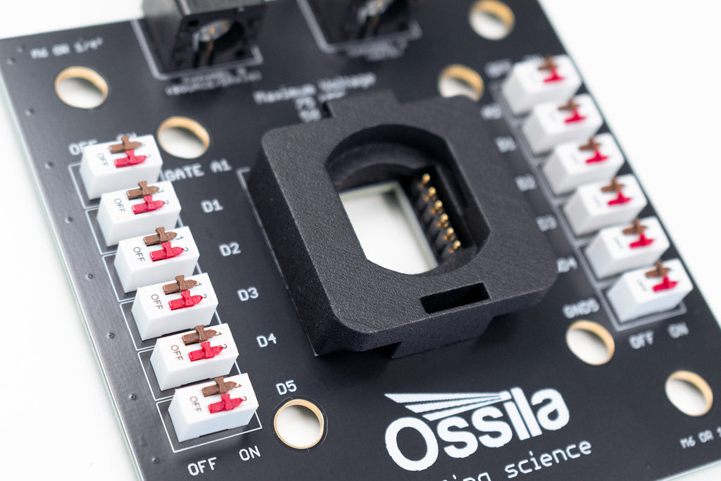
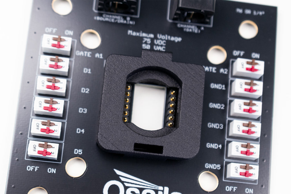
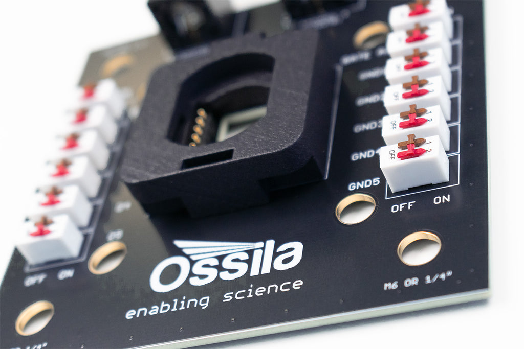
The Ossila Low Density OFET Test Board has been designed in tandem with the Ossila pre-patterned ITO OFET substrates (S161) and Silicon Oxide OFET Substrates, so that finished OFETs can simply be dropped into the testing slot with a push-fit connector. Switches control the connections to the five individual OFETs on a substrate, allowing device testing at the flick of a switch. Two BNC connectors make it easy to connect the source-drain and gates to a wide array of test equipment with a common earth (used to eliminate ground-loop currents). An optical window allows access for photosensitivity, photodoping and sensing measurements and metric/imperial mounting holes are provided for use with standard optical tables. The entire board is also compact at just 100 mm square to allow for easy use in a glove box.
Typically, OFET measurements are made using two source-measure units, with one used to set the gate voltage and measure any gate leakage current and the second used to sweep the source/drain voltage and measure the current. The termination terminal (drain/source for n-type/p-type respectively) is then usually grounded.
The Ossila Interdigitated ITO substrates (S161) contain five OFETs with individual source-drain connections and a common gate contact. The substrate is contacted by gold-coated, spring-loaded connectors with a push-fit lid (used to ensure that there is an easy and reliable electrical contact). This product is covered by our FREE 2-year warranty.

The test board has been designed with maximum experimental versatility in mind, and has the following features:
- Twin BNC connectors for easy connection to source measure units (SMUs). Channel B is used for the source or drain connection while channel A measures the gate connection.
- The Drain and Gate share a common ground which has the advantage of eliminating any earth-loop currents that can otherwise be formed - important for nanoamp range measurements.
- Gate connection switches to activate the gate connection to Channel A. A common gate is used for all five OFETs.
- Device sense switches to connect the source (n-type) or drain (p-type) contacts of the five individual OFETs to Channel B.
- Optical window for experimental access. Can be used to either illuminate devices for sensing/doping experiments or microscope inspection or a wide array of optoelectrical measurements.
| Substrate Compatibility | |||||
 Suitable for 20 x 15 mm substrates |
|
||||

