Patterned ITO Substrates for Rapid OLED and PV Prototyping
Large pixels for record breaking-devices
Transmittance | Characterization | Related Products | Resources and Support
The 25 mm square substrates have been designed to help the community take the next step in scaling up active areas. When combined with our deposition masks, these substrates allow four pixels per substrate, with active areas of 48 mm2 each, or a single large pixel with an active area of 255 mm2.
Specifications
| Substrate Size | 25 mm x 25 mm |
|---|---|
| Thickness | 1.1 mm |
| Glass Type | Polished soda lime, float glass |
| Substrate Coating | Fully oxidized ITO |
| ITO Thickness | 100 nm |
| ITO Resistance | 20 Ω / square |
| Glass Roughness | < 1 nm RMS (By AFM) |
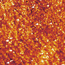
| ITO Roughness | 1.8 nm RMS (By AFM) |
| Pixel Sizes | 48 mm2 (6 mm x 8 mm) or 255 mm2 (15 mm x 17 mm) |
Transmittance of ITO Substrates
Characterization


Related Products
Resources and Support
 OLED Fabrication Guide
Fabricating OLED devices using Ossila’s pre-patterned ITO substrates is designed to be quick and easy. We've included every detail that we can in this manual so that you can produce efficient devices with as little effort as possible.
Read more... OPV Fabrication Guide
Within this guide, you’ll find comprehensive explanations for each step, along with additional tips and insights we’ve gathered to help you achieve the best possible results.
Read more... Transparent Conductive Oxides
Transparent conductive oxides (TCOs) are metal oxides, such as zinc oxide and tin oxide, that are capable of conducting electricity whilst being optically transparent. Find out about the chemistry behind ITO and why it is so popular.
Learn more...

