Platinum OFET Test Chips (High Density)
Robust, Reusable Test Chips For Quick OFET Screening
Patterned with photolithography for very narrow channel lengths, and high density design for better statistics
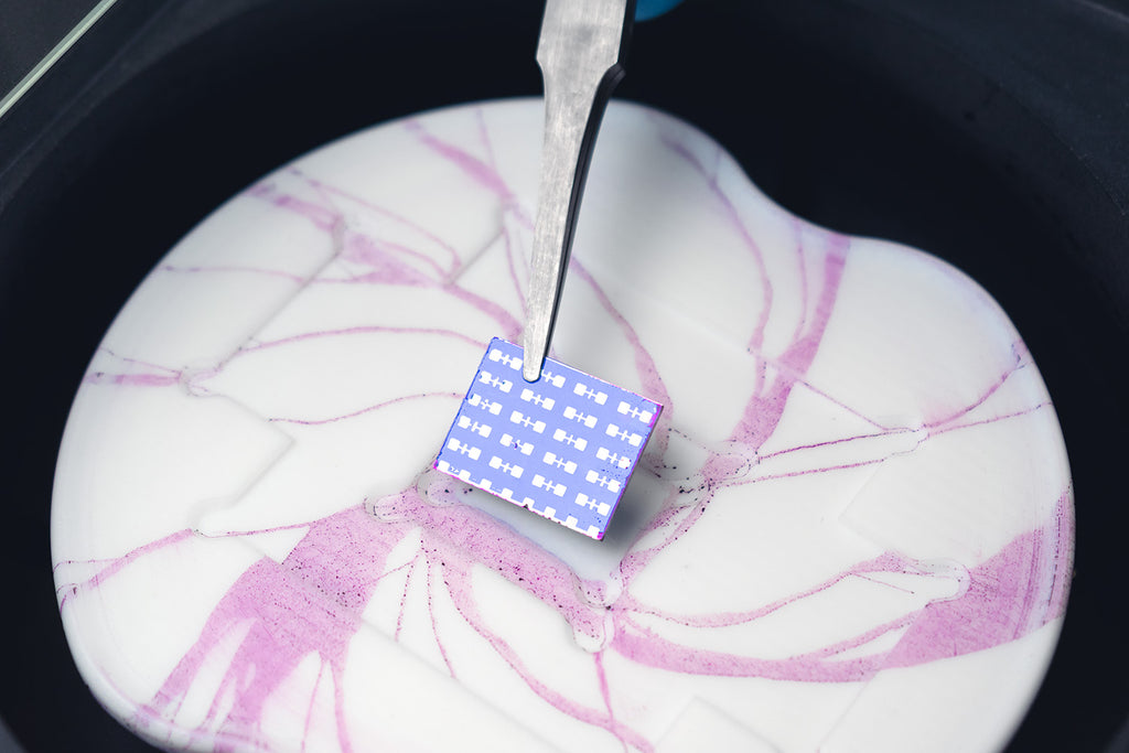
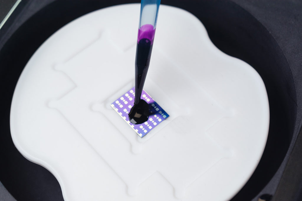
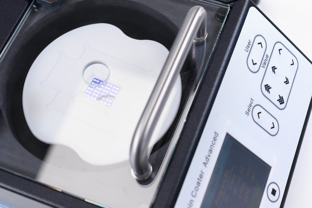
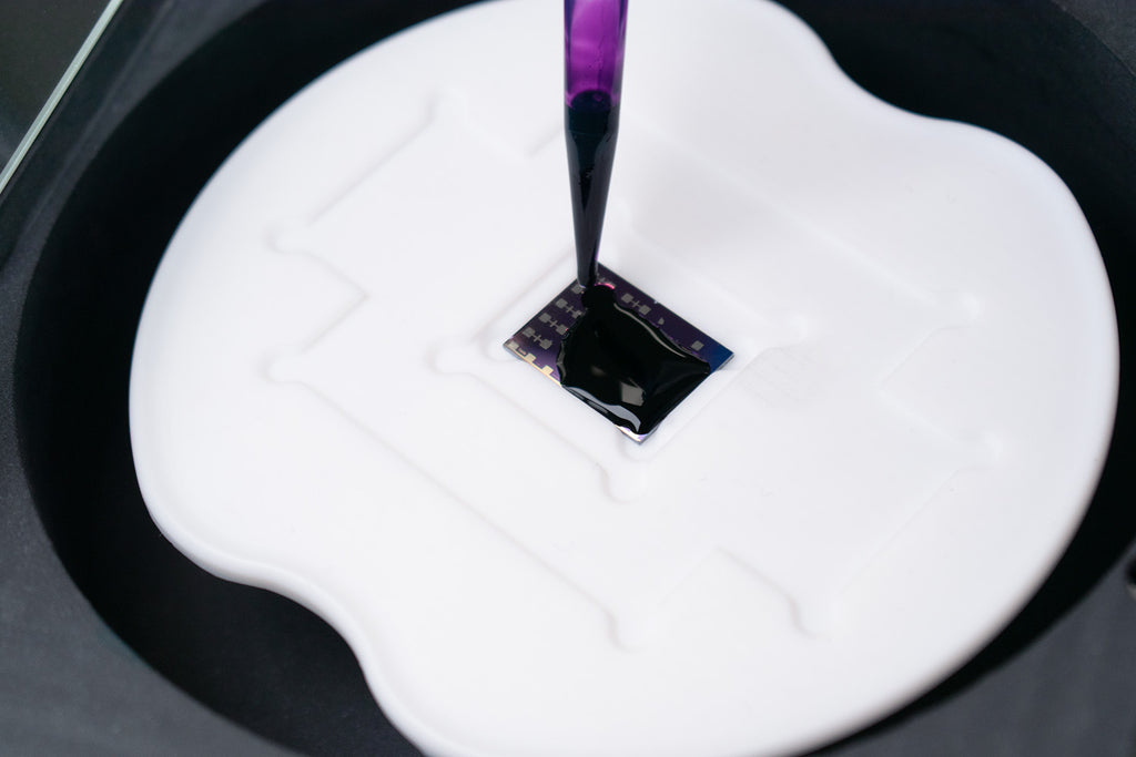
Simply coat your organic layer and start testing, with the platinum OFET Test Chips. The platinum is sputtered onto a titanium adhesion layer, providing an extremely robust contact and channel that can withstand solvent sonication, plasma etching, and swabbing. These test chips are designed to be reused multiple times for testing various materials, saving researchers time and money.
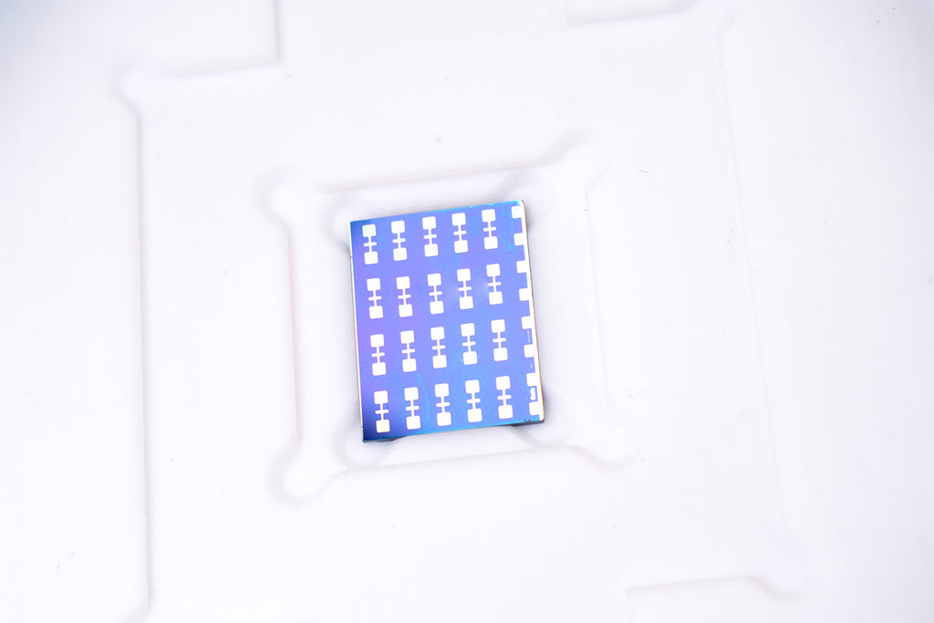
Mobility screening is made quick and simple with our prefabricated high density test chips. Create up to 20 OFET devices by coating one semiconductor layer. In addition, using our high-density OFET test board, you can test the entire chip in as little as 3 minutes reducing the overall time of both fabrication and measurement.
| Product code | Channel geometry | Channel width | Channel length | Electrode pairs | Quantity | Price |
| S403A1 | Linear | 1 mm | 2-10 μm Variable | 20 | 1 | £150 |
| S403A2 | Linear | 1 mm | 4-10 μm Variable | 16 (minimum) | 1 | £90 |
Looking for prefabricated OFET test chips on silicon/silicon oxide substrates?
We have discontinued our prefabricated OFET test chips on silicon/silicon oxide substrates (high and low density). If you are not sure if our newer reusable platinum OFET test chips will be suitable for your application, please contact us for advice.
Specifications
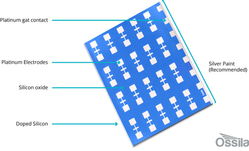
We fabricate our platinum test chips from p-doped silicon substrates. An insulating 300 nm silicon oxide gate dielectric is first grown on both sides of the silicon. The source and drain contacts consist of a 5 nm titanium adhesion layer below 100 nm of platinum. A platinum gate contact is also deposited along one edge of each substrate.
NOTE: Patterning using photolithography leaves exposed edges of the titanium adhesion layer. The consequence of this is that charge injection into the semiconducting layer can occur from the adhesion layer boundary instead of the platinum. Therefore these devices are recommend for single-crystal or single-flake materials that can sit on top of the electrode and span the electrode gap.
It is essential that there is an electrical connection between the gate contact and the p-doped silicon on the substrate sides. When the substrates are diced, a weak electrical connection is formed, however this can be easily removed when cleaning the substrate. We recommend applying silver (conductive) paint along and around the gate contact edge so that a more robust connection is made with the substrate edge.
For individual details and dimension drawings of each substrate type see below.
Linear variable channel length substrates (S403A1 & S403A2)
| Geometry | Linear |
| Arrangement (S403A1) | 20 electrode pairs, 5 channel widths |
| Arrangement (S403A2) | 16 electrode pairs minimum, 4 channel widths minimum* |
| Channel width | 1 mm |
| Channel lengths | 2 (S403A1 only), 4, 6, 8, and 10 µm |
*Please note that the fabrication and layout of S403A1 and S403A2 is identical, however one or more of the 2 µm channels may not be fully resolved on the S403A2 substrates (as highlighted with the red dotted border in the figure below). All four 2 µm channels are present on the S403A1 substrates. The S403A2 substrates may have some cosmetic defects (edge chips, minor surface scratches) that will not affect device performance.

Characteristics


| Substrate / Gate | Silicon (p-doped) |
| Gate dielectric | 300 nm thermally grown silicon dioxide |
| Source-Drain electrodes | Platinum (100 nm) / Titanium adhesion layer (5 nm) |
| Deposition method | Plasma sputtering |
| Patterning method | Photolithography |
Applications
Ossila High Density Substrates feature up to 20 OFETs on a single chip. This method of material screening is beneficial for several reasons.
- Experimental or production costs are reduced. By producing a higher volume of OFETs per substrate compared to the low density equivalents, you can increase statistics with fewer device runs. Also, the reusable design of these chips mean these substrates can be washed and re-tested rather than thrown away after use. This can help to stretch your budget to allow you to produce and test larger numbers of OFETs.
- This methods makes producing OFETs a far faster and less laborious process. Fabrication time is reduced by up to 50% when using prefabricated high density OFETs, freeing up more time to test the devices. As a result of this, greater volumes of data can be produced which in turn can provide more robust and reliable research.
- OFET variability is reduced since a larger number of OFETs are produced with each fabrication. At Ossila we have optimized the fabrication process in order to produce consistently high quality substrates. In this respect, using our prefabricated substrates rather than fabricating your own can help you to gather more reliable data to benefit your research project.
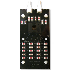
Prefabricated high density substrates are ideal for mobility testing as they enable swift, efficient testing of high volumes of OFETs. The Ossila high-density OFET test board has been designed specifically to test this device architecture, further quickening the process.
Rather than using a mechanical probe station to test OFETs, which can be delicate and time-consuming, the high density test board allows testing of multiple OFETs at one time. Simply drop the substrate into the test slot, secure the push-fit lid and connect the board via its BNC connectors to an array of test equipment.
The board has been intelligently designed to reduce external noise, leakage current and stray capacitance in order to provide reliable and precise low-current testing.