OFET Test Board for High Density OFETs
Achieve more reliable, statistical results.
Provide high precision, current-voltage measurements of up to 20 OFETs on a single substrate
The High Density OFET Test Board can provide high precision, current-voltage measurements of up to 20 OFETs on a single substrate. As such, this test board can speed up your research and help you to achieve more reliable, statistical results. It is compatible with our Prefabricated High Density OFET Substrates.
System overview
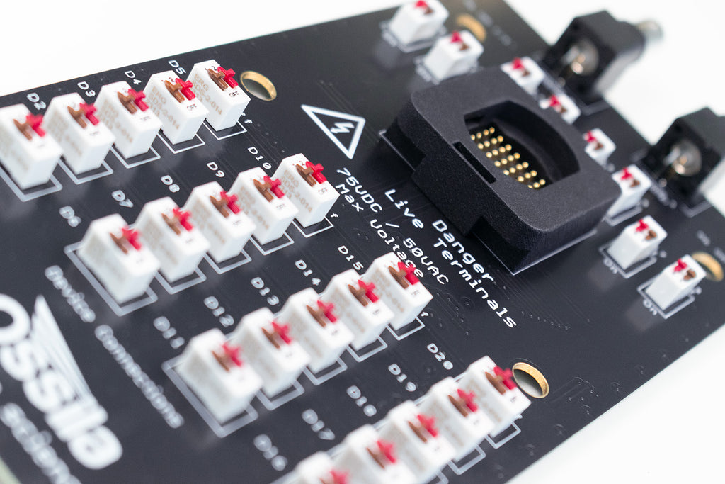
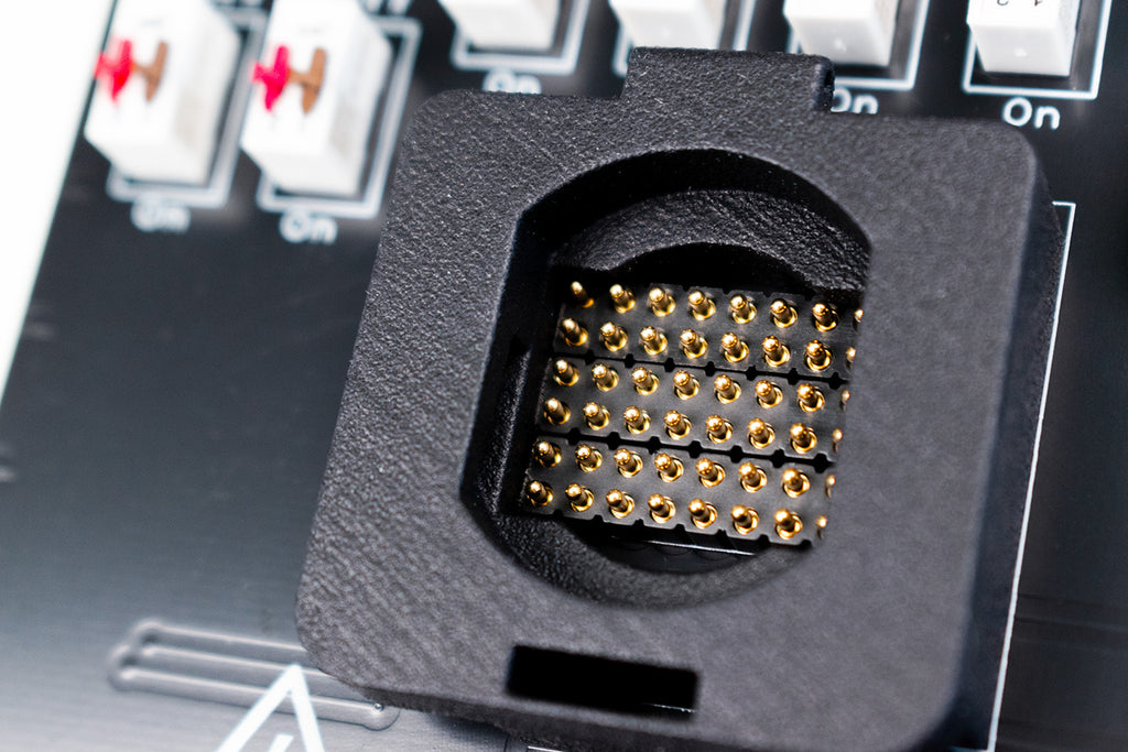
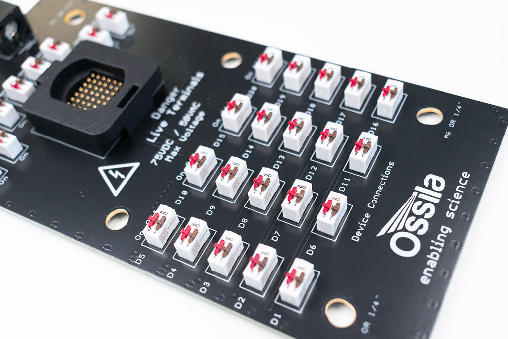
Until now, high density OFETs had to be tested using a mechanical needle probe station which was a delicate and laborious process. The substrate bracket on this board features 20 gold-plated, spring-loaded pogo connectors to make a reliable electrical contact with each device on the substrate. Not only does this make the testing process simpler and faster, but it also ensures uniform electrical contact with every single substrate tested.
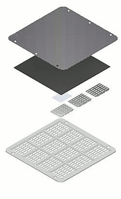
The substrate to be tested is simply dropped into the testing holder and secured in place with a swivel push-fit lid. The optical window then provides access for photosensitivity, photodoping and sensing measurements if needed.
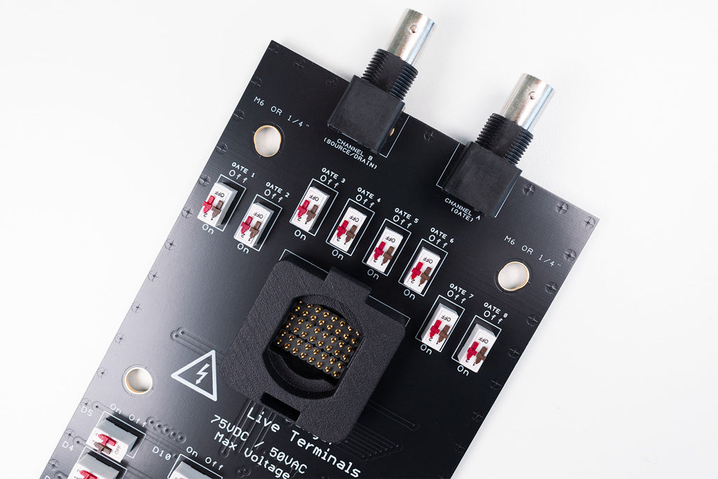
OFET measurements are made using two source measure units (SMUs) connected via BNC connector cables: one to set the gate voltage and measure any gate leakage current; the second to set the source-drain voltage and measure the current.
The board is also neat and compact at just 200 mm2 which is small enough for easy use within a glove box. This product is covered by our FREE 2-year warranty.

Features and Specifications
| SMU connection | Twin BNC connectors: Channel B = source/drain connection; Channel A = gate connection |
|---|---|
| OFET connection | 20 gold-plated, spring-loaded pogo connectors |
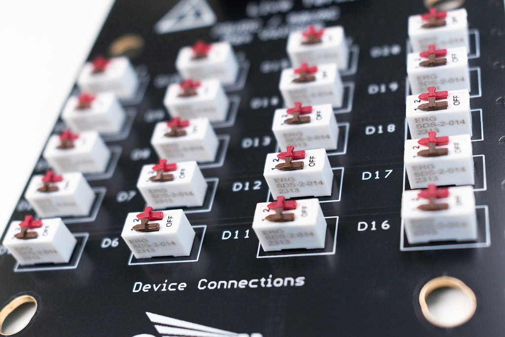
| Source-Drain switches | 20 independent switches to Channel B; one per device. |
| Gate switches | 8 independent switches to Channel A |
| Optical window | For experimental access: optoelectrical measurements; device illumination (sensing/doping); microscope inspection |
| Dimensions (L x W) | 200 mm x 100 mm (7.87" x 3.94") |
Noise reduction and electrical isolation
The High Density OFET Test Board has been designed to reduce non-negligible error, which often occurs as a result of stray capacitance, electromagnetic noise and difficulty isolating the test components (BNC cables, switches, board). Our test board has the following features to enable precision low-current measurement:
- Double ground plane – to reduce electromagnetic pickup from the environment
- Intelligent wire tracks – designed to reduce noise, leakage current and stray capacitance
- “Ideal” switch selection – proven to show almost no extra resistance to current flow when ON, and does not introduce leakages current when OFF
Compatible Products
The High Density OFET Test Board has been designed to be compatible with our Prefabricated High Density OFET Substrates.
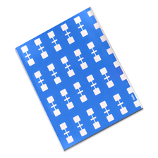
Prefabricated substrates can reduce OFET fabrication time - simply deposit your semiconductor on top - making them ideal for high throughput screening where reliable statistics are required. The High Density OFET substrates in particular allow for statistical data to be collected, with reduced variability between OFETs and reduced cost and processing time per OFET device with 20 devices on a single substrate.
If you prefer to fabricate your own OFETs, you can use our high density OFET fabrication system which contains all the relevant components needed including substrates, interchangeable masks, lower support and lid.
| Substrate Compatibility | |||||
 Suitable for 20 x 15 mm substrates |
|
|
|||