


Thin Film Characterization
Thin films are used in solar cells, protective coatings, light emitting devices, flexible sensors, device interlayers, lasers, thin film transistors and many more applications. Therefore, it is vital to be able to precisely deposit and accurately characterize these films.
To thoroughly characterize a thin film, you will need to examine the film’s morphological, structural and molecular properties, along with (in some applications) optical, electrical and chemical characteristics. As you will see, a lot of these properties inform and depend on each other, so you will need multiple techniques to build a full picture.
In any thin film research, it is important to have the right toolkit of measurements and methods. This page will outline some of the key methods used to measure thin films, highlighting their benefits and limitations. While this is not an exhaustive resource, this overview is a great place to start when learning about thin film characterization.
Contents
- Thin Film Properties
- Optical Properties
- Morphological and Topographical Properties
- Intrinsic Structure
- Film Thickness
- Mechanical Properties
- Elemental Analysis
- Thin Film Characterization Techniques
- Ellipsometry
- Surface Profilometer
- Atomic Force Microscopy
- Scanning Electron Microscopy
- Spectroscopy Techniques
- Contact Mechanics
- Application Dependent Measurements
Thin Film Properties
Optical Properties
Optical characterization uses techniques that explore how a thin film interacts with light.
The movement and behaviour of light within or around thin films depends not only on the wavelength of light, but also on the thin film properties themselves. Choice of material, morphology, crystal structure and film thickness can all affect a film's optical properties. For these reasons, the optical properties of a thin film can vary drastically from those of the bulk material, so you may need to measure both.
Optical probing techniques (such as spectroscopy) are easy, non-invasive measurements that are generally suitable for thin films. Measuring different optical properties requires different types of optical spectroscopy measurements (absorbance, fluorescence, time-resolved spectroscopy, refractive index, etc). Some examples are listed in the table below.

| Application | Requirement | Measurement |
|---|---|---|
|
Non-active layer in light activated device e.g. electrode in a solar cell/LED Some protective coatings. |
High transmission in the visible region | Transmission spectrum |
|
Non-active layer in light activated device i.e. electrode in a solar cell/LED Some protective coatings. |
Smooth transition between layers/into surrounding medium | Refractive index |
| Solar cell material | High absorbance across the visible region | Absorbance spectrum |
| Active layer in light sensing device | High absorbance in the region of interest | Absorbance spectrum |
| Active layer in light emitting devices | High emission within the region of interest | PL/fluorescence measurement |
You can also use optical techniques to probe other thin film properties, such as:
- Semiconductor band gaps
- Concentration of a fluorescent material in solution
- Stoichiometry
- Aggregates, complexes and impurities
- Glass transition temperature in polymer films
- Film heterogeneity

Morphological and Topographical Properties
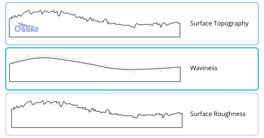
Morphology refers to the physical structure (e.g. grain size/shape) and surface roughness of a thin film. Techniques that measure surface roughness and waviness, such as surface profilometry and atomic force microscopy, will highlight macro- and micro-properties of the film, such as overall thickness variation, local height fluctuations, grain size or overall distribution of blends across a film.
Here are some examples of how these properties can impact both the integration of a thin film in a device, and its qualities as a standalone coating:
- Often, thin films are sandwiched between other thin films. In these cases, each layer needs to be smooth and uniform to ensure consistent high-quality layer deposition.
- In other cases, films need to have strong adhesion properties so benefit from a rougher surface.
- Also, some films, such as polymer blends, need to sacrifice some layer smoothness to increase another property (e.g. to increase surface area or to create good mixing). In some cases, it’s a balance of maximizing film uniformity without sacrificing this other property.
- Surface roughness measurements can highlight issues with your deposition method or inconsistent substrate heights.
Intrinsic Structure
Here, intrinsic structural measurements are techniques that examine a film’s structure below the surface. This could involve examining the film’s crystal structure, its internal morphology and the distribution of different phases throughout the film.
For example:
- If working with inorganic crystals, the crystal structure will affect many other properties of the thin film such as its thermal and electrical conductivity, stability and structural properties.
- Alternatively, when mixing multiple materials in a blended thin film, intrinsic structural measurements can tell you if the materials truly blend or if they stay as separate phases within the film.
X-ray scattering techniques, such as X-ray diffraction (XRD) and grazing-incidence wide angle X-ray scattering (GIWAXS), can be used to examine the internal structure of a film.
Film Thickness
Accurately measuring film thickness is vital for characterizing many thin films. Thickness affects the structural properties of the film and is strongly related to its optical properties (according to Beer Lambert's law). A film’s thickness can also impact the colour of the film and is critical for optical cavities and laser applications.
Thin film thickness can be measured with step-height techniques, such as a stylus profilometer, or through optical techniques like ellipsometry.
Mechanical Properties
Mechanical properties are properties that affect the overall structure of the film (hardness, Young’s modulus, bendability, flexibility, etc). Ensuring mechanical stability in thin films is important, especially for flexible electronics and various biosensors.
As well as specific applications, any thin film, whether used for protective coatings or an interface layer, should be able to withstand standard operational conditions, so ensuring your thin film doesn’t break under operational movement at working temperatures is an important consideration.
The high surface-to-volume ratio of thin films means they are quite susceptible to structural failure due to small defects, especially those introduced during fabrication. This can induce strain and stress in a film that can turn microstructures into serious structural issues.
Mechanical testing of thin films is often difficult, as these films are more fragile than traditional testing methods allow. However, bending cycling, crack onset strain measurement and plane-strain bulge testing are some of the methods that test thin film flexibility and durability.
Elemental Analysis
Elemental analysis maps how elements are distributed across a thin film's surface or through its depth. This can highlight any defects or instabilities, give insight into the deposition process, and show how evenly materials are spread or how well components have blended.
For example, if integrating dopants or passivating materials into your thin film, it is important to probe how these are distributed within the film. In some cases, even spread of these materials improves the performance of the whole film. Passivating materials, by contrast, may be intended to target specific regions such as grain boundaries, and elemental analysis can confirm they are localized there.
Measurements that probe elemental distribution include X-ray Photoelectron Spectroscopy and SEM-EDS.
Thin Film Characterization Techniques
Ellipsometry
Ellipsometry uses the change in polarization of light after it is reflected off a specular thin film to measure its refractive index and thickness with high accuracy. It does this by measuring the complex reflectance ratio from which you can extract these thin film properties by applying an optical model.
If ellipsometry is used appropriately, it can be an extremely accurate technique, achieving sub-nanometer resolution. It is also a useful technique for measuring properties of ultra-thin films. Additionally, its non-invasive nature makes this a favorable technique for measuring the thickness of delicate or soft, smooth films.
However, there are certain restrictions on what samples you can accurately measure with ellipsometry. It is difficult to do ellipsometry on rough or textured thin films. . In fact, this technique requires <1 nm variation across the sample. Furthermore, transparent substrates like glass will introduce optical effects that can hinder ellipsometry measurements. The other difficulty with ellipsometry is that you need to apply the right model, otherwise the extracted information will be useless.
Surface Profilometer
Surface profilometers are systems that map the surface profile of a thin film. The two main types of profilometer are stylus profilometer and optical profilometer.
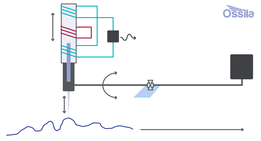
Stylus profilometers record the vertical deflection of a stylus as it is moved across a surface. Tracking this movement creates a line profile representing the surface’s features. The stylus is kept in contact with the surface throughout this process, usually by maintaining a constant force. Stylus profilometers can measure features from 10 nm – 1 mm and can support a wide range of substrates. However, resolution is limited by the stylus tip diameter, since a tip that's too large can't resolve fine features (an effect known as tip convolution). Additionally, the tip could damage delicate samples if the force used is too great.
Optical profilometers use reflected light to track surface morphology. These profilometers focus light onto the surface and use changing interference patterns, focus variation or light deflection to map the vertical profile of the sample. It is a non-contact method so there is no risk of damaging the sample. However, you need to know the sample's optical properties before measurement, and this system struggles with rough or highly reflective surfaces.
Profilometry is commonly used to measure the step heights of patterned surfaces created by atomic layer deposition, lithography or etching methods. In these cases, accurate patterning, consistent layer thickness and sharply defined edges are critical to device performance.
Some systems can also quantify surface roughness and waviness (via parameters like Ra, Rz, and Rmax), which can flag issues like inconsistent deposition or surface contamination.
Atomic Force Microscopy
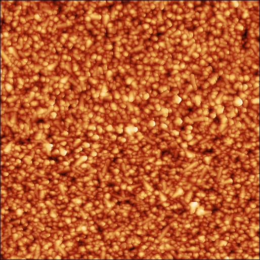
Atomic force microscopy uses a similar approach to stylus profilometry. It uses a small tip (< 10 nm in diameter) attached to a cantilever. As the probe moves across the surface, the tip either makes direct contact with the sample or measures Van Der Waals forces as the tip approaches the surface. This interaction with the sample is translated into a height profile, and these line profiles can be used to build a topography map. It can also measure surface roughness values with high accuracy (albeit over a much smaller area than profilometry can measure).
AFM can take very high-resolution height profiles of thin and delicate samples, such as biological samples and polymer films It can also be combined with other techniques to correlate physical features with other properties e.g. photoconductive AFM , STORM AFM, etc. It can be used to study a wide range of length scales, from 10 µm to subnanometer features.
However, AFM measurements take a long time (compared to measurements like SEM) and requires close contact or interaction with the sample which can cause damage if contact mode or excessive force is used. Also, AFM has a limited height range, so cannot be used to measure very rough samples or tall features. Finally in part, AFM's resolution is inversely proportional to scan length, so measuring the finest details often requires smaller scan areas (less than 1 µm x 1 μm). Therefore, you must measure several spots over the surface to characterize a thin film completely.
Scanning Electron Microscopy
Scanning electron microscopy is a technique which exposes a sample to a charged electron beam and measures the secondary and backscattered electrons emitted from the sample. This technique can overcome the diffraction limit, producing very detailed images of a thin film’s surface.
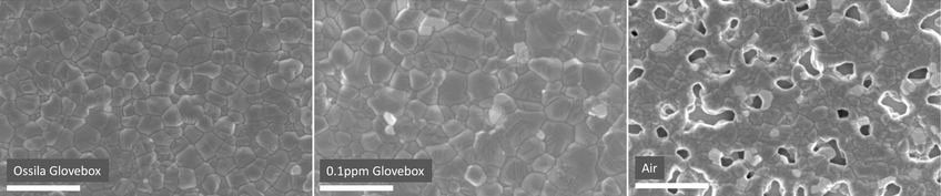
This technique produces a clear scan with a similar image resolution to AFM. It’s also much faster than AFM, and you can image with high resolution over relatively large areas. Additionally, cross sectional SEM can be used to image multiple layers of a device at once, allowing insights into both the layers and the interfaces between them. You can also use SEM-EDS to not only image your sample but also probe elemental distribution through your sample.
The main limitation of SEM is the surface you are imaging must be conductive and robust. If the sample isn’t conductive, you must coat the film in a thin layer of gold or other conductive material. Furthermore, the gold coating can damage delicate samples. Alternatively for delicate conductive surfaces, the electron beam can destroy the surface while imaging.
SEM is ideal for imaging conductive features on a thin film , analyzing multilayer devices and probing growth mechanics of a crystalized thin film.
Spectroscopy Techniques
Visible spectrophotometry is one of the quickest and most accessible ways to probe a thin film. This involves exposing your thin film to visible light and measuring the light that is transmitted or emitted from the surface.

- Absorbance measurements can provide a molecular fingerprint of a thin film, helping to identify, quantify and track chemical species in your thin film.
- Absorbance and transmission measurements are especially important if the thin films require specific optical properties, such as high transparency (window coatings or thin films used in as transport layers in optical devices).
- Accurate emission characterization is critical for fluorescent thin films to be used in LEDs and other fluorophores.
- On top of this, absorbance measurements can be used to identify contamination in your film or to probe the thickness of a layer through Beer Lambert’s law.
This technique is best suited to qualitative rather than quantitative measurements. You can extract a lot of useful information out of spectrophotometry measurements, but it requires careful sample preparation, analysis and appropriate reference measurements. However, this technique is only useful for samples that interact, emit or (are thin enough to) transmit visible light.
Also, for transmission measurements, you need to put your film on a transparent sample such as glass or transparent plastic.
Application Dependent Measurements
As well as general thin film properties, further measurements are often necessary for specific applications. These determine the suitability of a film or stack for that specific application.
Electrical Measurements

One of the most important measurements for electronic devices is thin film conductivity. In thin films, sheet resistance is the most commonly used metric.
Conductivity can be measured using a range of techniques. You can measure conductivity by simply applying a voltage between two points. Users can do this with a standard multimeter or using micromanipulators.
However, four-point probe measurements are the standard in most thin film research. This uses four equally spaced probes. The outer probes apply a current across the film, while the inner two probes measure the voltage drop between them. This is better than simple two-point conductivity measurements as it eliminates contact and wire resistance, making sheet resistance measurements more accurate.
Current-voltage sweeps are another fundamental measurement used to assess electrical properties of a device. This measurement plots a characteristic curve and from this, distinguishing features of many electronic devices can be identified including:
- Resistance of resistors.
- Threshold voltage, on/off ratio and subthreshold slope of field effect transistors.
- Turn on voltage and current efficiency of light emitting diodes.
- Open circuit voltage, short circuit current, fill factor and subsequently efficiency of solar cells.
I-V curves are typically measured using source measure units connected to testing board or test system.
Biocompatibility
This can mean many things depending on the intended application of the film, but for proof-of-concept experiments biocompatibility experiments, biocompatibility tends to mean:
- Is the material stable in water-based solutions?
- Is the material non-toxic?
To assess the toxicity of a material in a system requires a series of in-vivo and in-vitro experiments. This can test if the material causes inflammation, irritation or affects cell processes.
Furthermore, thin films used for biosensors often need to be flexible and stretchable to make efficient contact with non-standard substrates (such as skin or organic tissue).
Electrochemical Measurements
In some cases, it is necessary to assess how a film interacts with an electrolyte rather than just air. This is particularly key for protective coatings, biosensors and any films with electroactive or redox-active components.
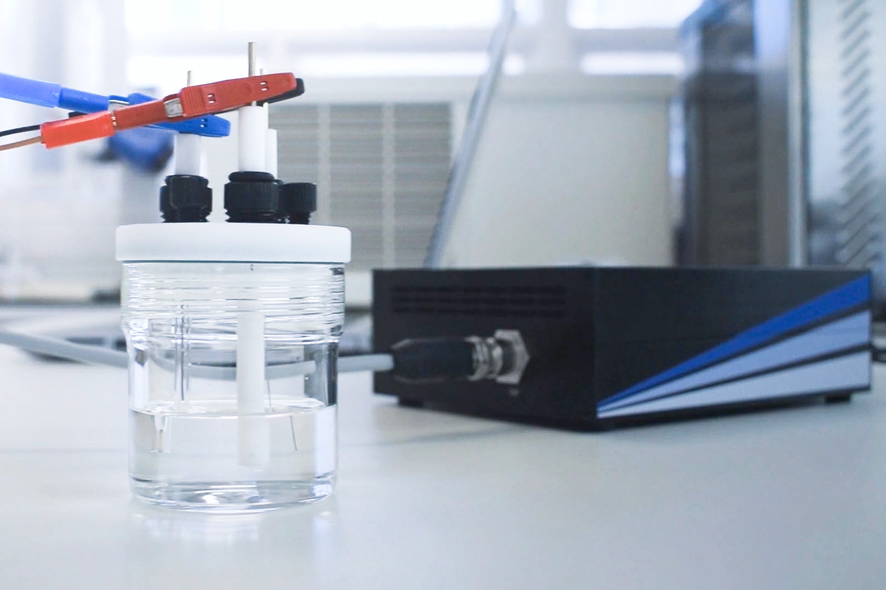
Cyclic voltammetry (CV) is one of the most common techniques used for this. Using a three-electrode setup (working, counter and reference electrodes), the working electrode's potential is swept cyclically against the reference and the resulting current is measured. By coating the working electrode in the material of interest, you can produce a current-voltage curve that reveals redox behaviour, electroactive surface area and the electrochemical stability window of the film.
Electrochemical impedance spectroscopy (EIS) is another technique used to investigate the electrical and interfacial properties of a thin film and an electrolyte. It applies a small AC voltage of varying frequencies across the film-electrolyte interface and measures the resulting impedance. This is particularly useful for protective coatings, as it can reveal defects, pinholes, charge-transfer resistance and barrier properties without damaging the film.
For coatings specifically designed to resist corrosion, open-circuit potential (OCP) and potentiodynamic polarization measurements can help determine corrosion potential and corrosion rate, to predict how well a coating will protect an underlying substrate over time.
References
- Tunable Structural Color Images by UV-Patterned Conducting Polymer..., S. Chen et al., Advanced Materials (2021)
- Flexible Electronics: Status, Challenges and Opportunities., Corzo D, Tostado-Blázquez G and Baran D, Front. Electron (2020)
- Quantitative characterization of thin-film cracking behavior enabled by..., H. Hu eta= al., Thin Solid Films (2023)
- Plane-strain Bulge Test for Thin Films, Y. Xiang, X. Chen & J.J. Vlassak, J. Mat. Res. (2005)
- Determination of refractive index and layer thickness of..., P. Nestler & C.A. Helm, Opt. Express. (2017)