Stylus Profilometers Working Principles
Jump to: How Does A Stylus Profilometer Work? | Optical Vs. Stylus Profilometers | Measuring Step Heights | Roughness Measurements
Stylus profilometers can be used for a wide range of measurements, including surface feature characterization, measuring the step heights of patterned surfaces, assessing thin film thicknesses and for surface roughness or waviness measurements. Profilometer techniques are a staple of any thin film characterization toolbox.
A typical stylus profilometer can measure features and step heights ranging from 10 nm - 1 mm. Stylus or contact profilometers use a stylus to trace across the sample surface. This is in contrast to optical profilometers, that use light reflections to map changes in surface topography.
How Does a Stylus Profilometer Work?
The stylus profilometer head has three main components:
- Stylus
- Transducer Element
- Arm and Counterbalances
In a stylus or contact profilometer, the stylus makes vertical contact with a sample. As it moves across a sample, the tip must move up and down to maintain a set height and force between itself and the sample surface. The deflection of this stylus is measured. The flexible movement of the stylus in the z direction is facilitated by a frictionless pivot. The profilometer must also contain components to reduce the amount of force placed on the sample.
This profilometer head is connected to external processing electronics. These systems also require a moveable stage in order to navigate and scan across a sample.
Stylus and Arm
The stylus design, specifically the tip design, will significantly affect your scan quality and resolution. The tip size will always limit the feature size you can study, therefore the resolution of the scan. One example of this effect is shown in this image, where the stylus tip is too large to measure the detail of the smaller depressions with any resolution.

This is known in atomic force microscopy as tip convolution, but this concept is also relevant to surface profilometry. Tip convolution occurs when the radius of curvature of the tip is similar to or larger than the feature being measured. In these situations, the sides of your tip come into contact with the feature before the tip apex, leading to a broadening of feature size.
Tip damage can also have a significant impact on surface profilometry measurements. Using smaller tips may increase the resolution of your measurement, but smaller tips are more easily damaged. This will limit the amount of force you can place on your stylus without deforming it. However even with careful use, tips will become blunted or damaged over time. If you're not careful with this, your image resolution may begin to deteriorate, leading to inaccurate measurements.
In order to trace over a surface, the stylus must be able to move fluidly in the z direction, while having as little impact on the surface as possible. To facilitate this fluid movement, the stylus is attached to an arm that extends through a pivot point which is attached to a frictionless pivot. This configuration acts as a classical spring mass system.
We must also consider and control the potential force that is exerted on the surface by the profilometer itself. To control the force that the stylus-tip exerts on the surface, we must consider three components:
- Counterbalancing the weight of the cantilever and tip so that little or no gravimetric force is applied by the tip to the surface while it is in the neutral position.
- Compensating for the spring-constant of the pivot. Under normal conditions, this acts like a spring. As the stylus tracks the surface, it creates a restoring-force in the pivot, to move it back towards the neutral position. Magnets can be used to counteract this, creating a force approximately equal and opposite to the restoring force of the pivot's spring constant. One magnet is attached to the arm, and the other to the mounting-body. Changing the separation of these magnets will change their exerting force, until the restoring force is cancelled out.
- Creating a mechanism which can electronically control the force exerted by the stylus tip. This can be done using a magnetic solenoid.
Transducers and Feedback Systems
This is the component that translates physical movement to a measurable electronic signal. Multiple types of transducers can be used in profilometers.

Various mechanisms can be used to track this displacement.
- In capacitance sensors, the movement of the core changes the capacitance of a transducer.
- Piezoelectric transducers use piezoelectric materials to translate physical movement into electrical signals. The output current changes depending on the force pressing on the piezoelectric material.
- Inductive transducers use a moving core within a set of coils to alter mutual inductance, producing a voltage output that varies linearly with the core's displacement.
- Laser interferometer-based systems rely on laser alignment to measure height variation.
Optical Vs. Stylus Profilometers
Optical profilometers use light to characterize surface features instead of using direct contact. These systems can include laser, optical or confocal microscopy.
A light source is split into a reference beam and a measurement beam. The measurement beam is reflected off a sample and then compared to the reference beam. The superposition of in-phase and out-of-phase elements creates constructive and destructive interference patterns. A CCD array measures the light and dark areas, building a picture of how the light has been scattered by different structures on the sample.
For optical measurement systems, factors such as beam shape, and shape of substrate can affect the measurement. Crucially however, both the optical properties of the thin films and their structure must be known in advance of the measurement.
Stylus profilometry is a reliable and well-established technique. It is ideally suited for measuring hard substrates, including transparent or reflective surfaces, which cannot be measured with optical techniques. Stylus profilometry also copes well with rough surfaces and unknown materials.
Optical profilometry can have a higher accuracy and requires no physical contact so can be used for sensitive samples. However, optical techniques require prior knowledge of a material’s optical properties and only work for relatively smooth surfaces.
Other techniques for measuring film morphology and thickness include ellipsometry. These methods can give some of the best sensitivities. However, stylus profilometry is a direct measurement, which requires no modeling to extract physical parameters. Also, techniques like ellipsometry don't work for transparent or reflective surfaces and can be difficult for measuring multilayer stacks. Also, stylus profilometer measurements are not sensitive to reflectivity or color unlike optical methods.
Measuring Step Heights
Measuring step heights is one of the most critical uses of surface profilometers. This technique is often used to characterize patterned surfaces. Creating patterned substrates is incredibly important for a range of devices including OFETs. Incorrect patterning could lead to shorting, reduce device efficiencies or hinder device lifetime.

These patterns are created by lithography, atomic layer deposition, sputtering or other evaporation methods, and their accurate characterization is of the utmost importance. You need to be able to characterize a step height as cleanly as possible in order to accurately image substrates and device layers. For this reason, nanoscale step height standard is an important measurement standard used for atomic force microscopes and profilometers.
Surface profilometers can also be used to measure device thickness. By removing a small amount of your thin film material (even scratching off a small section with tweezers), you can use a line profile to measure step change between the coated and uncoated regions. By averaging these profiles over several regions of a thin film, you can get a pretty reliable measurement for thin film thicknesses. While this method is not recommended for extremely thin or inconsistent samples, it is often used to measure layer thicknesses of > 50 nm.

Roughness Measurements
You can use surface profilometry to measure surface roughness. Surface roughness is a useful measurement for evaluating thin film properties. Assessing surface roughness is important if you want to reduce friction in mechanical parts, improve coating adhesion or improve the interfacial layers of a thin film device.
Film homogeneity can be split into 3 parameters: lay, roughness and waviness. The lay represents any regular finish or pattern, and its orientation. This effect is usually created during surface manufacturing and is not that important in research measurements. Roughness refers to micro-fluctuations or "micro-features" present across a film or device, whereas waviness refers to macro-fluctuations across a surface or substrate.

There are several ways to quantify surface roughness (Ra, Rz, Rq).
- Roughness average or the arithmetic mean roughness, Ra, is the mean height difference assessed over several peaks away from the mean line.
- Rz, is the average height difference between the 5 highest and 5 lowest peaks over a given distance.
- Rmax is the distance between the highest and lowest peak point. This measures the extremes of roughness.
Waviness or warpage is also an important measurement, especially with regards to substrate preparation or planarization. Assessing warpage can ensure or improve surface flatness and prevent irregularities during later processing steps. Also, this can be used to characterize curved surfaces.
It is important to separate these two values when assessing surface metrology as they are often caused by different things. Waviness can indicate an issue with the deposition method, leading to an inconsistent film thickness. However, increased surface roughness can signify problems like phase separation, solution or surface contamination or problematic crystallization mechanics. If you are measuring roughness, you will need to measure and remove waviness from your measurement, as this will artificially affect your roughness values.
With accurate profilometry measurements, you can quantify and improve the quality and uniformity of your layers or coatings.
Explore Our Resources
 Thin Film Thickness Measurement: Instrument Comparison
Precise and accurate measurement of thin film thickness is important in a range of fields. In semiconductor manufacturing, optical coatings, photovoltaics, and biomedical devices, even small variations in thickness can significantly affect performance.
Read more...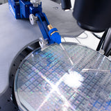 Semiconductor Characterization Methods
Semiconductor characterization refers to the process of measuring and evaluating the properties of a semiconductor. This is quite a broad term and can refer to different processes depending on the context. It can refer to:
Read more...
References
- Assessment of surface profile data acquired by a..., D-H Lee & N-G Cho, Measurement Science and Technology (2012)