Semiconductor Characterization: Methods for Materials and Devices

Material Testing | Electrical Characterization | Optical Characterization | Physical Characterization
Device Testing | Current-Voltage | Capacitance-Voltage | LEDs & Lasers | On-Wafer Testing
Semiconductor characterization refers to the process of measuring and evaluating the properties of a semiconductor. This is quite a broad term and can refer to different processes depending on the context. It can refer to:

- Characterization of new semiconductor materials in early development and R&D
- Characterization of a new semiconductor devices or component
- Characterization of industrially produced semiconductor chips fabricated on silicon wafers
All semiconductors have a characteristic band gap between 1-2 eV, which is useful for many different purposes (such as bipolar junction transistors, field-effect transistors, solar cells, LEDs, photodetectors, etc).
This also means there are many ways to characterize these materials. In order to characterize a semiconductor device or material thoroughly, you can use optical measurements, electrical measurements, morphological measurements, advanced imaging techniques or chemical probing methods.
The required characterization methods depend on the type of semiconductor, its intended application, the development stage of the technology and the available deposition techniques.
Electrical Characterization Equipment


Evaluating Semiconductor Materials
Semiconductors are integral to most modern electronics. Many materials fall under the semiconductor umbrella: crystalline silicon, thin film or amorphous silicon, compound semiconductors (e.g. Indium Arsenide, Gallium Arsenide, etc), organic semiconductors, some quantum dots, perovskites, some metal oxide nanoparticles and many more.
Determining the band gap of a material is only the start of choosing a semiconductor material. Depending on the application, the selected semiconductor, or "active material", will need to meet different requirements. Even if the band gap is right, you may also need to examine a material's excitonic and morphological properties, how easy it is to deposit, it's charge carrier properties or its optical response.
Electrical Characterization
One fundamental measurement for semiconductors is their electrical conductivity. There are two main methods to find this: two point measurement or four point measurements.
Two point measurements are the simple way to measure this. These can be done using a standard multimeter, or a probe station set up allowing for precise probe positioning on small scale devices. You can even get full systems, like the Ossila Electrical Characterization System, which can facilite many types of electrical measurements. This very simple method creates a bias between the two probes and measures the resulting current flowing between them. From this you can work out resistance. However, this method includes contributions from both the material’s intrinsic resistance and contact resistance at the probe interfaces, which can lead to inaccuracies, especially in thin films or high-resistance materials.

You can also use the kelvin probe method (also known as the four-point probe technique) to measure conductivity. In this method, two outer probes source the current while the inner probes measure voltage across the sample or component. This allows you to remove contact resistance , giving you a more accurate resistance or sheet resistance. This eliminates the influence of contact resistance and provides a more accurate value of the sample resistance or sheet resistance, particularly for thin films. Dedicated four-point probe systems can measure sheet resistance in thin films. Alternatively, probe stations can be configured to do kelvin probe measurements across a thin film or device component.
Another key measurement for semiconductors is the Hall Effect. This allows you to measure the carrier concentration in a semiconductor. Here an electric field is applied along one axis of a semiconductor (let's say the x axis), while a magnetic field is applied along a perpendicular axis (let say the z axis). The resulting Lorentzian force will drive the charge carriers to polar sides of the y axis in the material. If there is a slight imbalance of charge carriers this will create an electric field across the y axis, known as the Hall voltage.
The Hall coefficient is defined as:

Where RH is the Hall coefficient, p is the hole concentration, n is the electron concentration, and µ is electron/hole mobility.
The Hall coefficent can be measured directly according to:

where Jx is current along the x axis, Bz is magnetic field along the z axis and εy is the built up electric field along the y axis.
Optical Characterization and Spectroscopy Techniques
Optical characterization is especially important for optoelectronic devices such as PV, LED and lasers.
One of the simplest techniques you can use is UV-Vis spectroscopy. Using a dedicated UV-vis spectroscopy systems, like the Ossila Spectrofluorometer, you can learn a lot about a semiconductor material. Absorbance measurements are vital for photovoltaics, photodetectors and LED applications, and can be useful if you are making transparent or semi-transparent films. Fluorescence spectroscopy is an integral part of characterizing fluorophores used in LEDs or lasing materials. Plus, electroluminescence measurements are instrumental for testing LED efficiency. For lasing materials, you can measure the amplified spontaneous emission using a calibrated spectrometer while the laser is being optically pumped.
You can find a semiconductors band gap by measuring its absorbance coefficient. For a disordered or amorphic semiconductor, the absorbance spectra will have an absorbance edge, where absorbance drops off sharply. This represents the energy threshold, above which electrons can be excited from the valence band into a higher electronic state, crossing the band gap. From this, you can estimate the band gap using the following relationship :

Where α is absorption coefficient, hν is photon energy, Eg is band gap and γ is a constant (0.5 for allowed direct transitions and 2 for indirect transitions).
You can also find this data from a Tauc plot, where you plot α2 against hν. If you fit a linear trend to the linear region of your absorbance edge, the band gap will be the interception of this line with the x axis.

Other spectroscopy methods, such as Raman spectroscopy and X-Ray spectroscopy, can probe the molecular structure of semiconductors. This technique allows researchers to analyze the vibrational states of a semiconductor and probe the chemical composition of conjugated and organic semiconductors. This can also be used to measure impurities in silicon semiconductors or assess stress in amorphous silicon films . Other scattering techniques such as X-ray diffraction, can probe the chemical composition of a material and examine crystal structure for crystalline semiconductors.
Physical Characterization
The physical characteristics of a semiconductor will be important in any semiconductor device. If films are solution processed, their wettability, surface tension, crystallization and drying mechanics and solution properties can massively affect the final film. On the other hand, many semiconductor layers are deposited via evaporation methods, where layer morphology and thermal stability become primary concerns.
Depending on the application, there may be other conditions imposed on the semiconductor. For example in flexible electronics, mechanical properties like tensile strength and elasticity are especially important. Additionally, different semiconductors will have different growth mechanics and film morphology that can impact their electrical performance.
To evaluate these materials in thin films, surface characterization techniques like atomic force microscopy (AFM), surface profilometry and scanning electron microscopy (SEM) are commonly used. These methods enable surface roughness measurements and can help visualize effects like phase separation or different crystallization regions within a film.
If you are making quantum dot devices, it is important to accurately characterize their size and shape, as this can really affect their electronic and optical properties. You can use techniques like dynamic light scattering, UV-Vis spectroscopy or TEM to characterize nanoparticle size.
Testing Semiconductor Devices
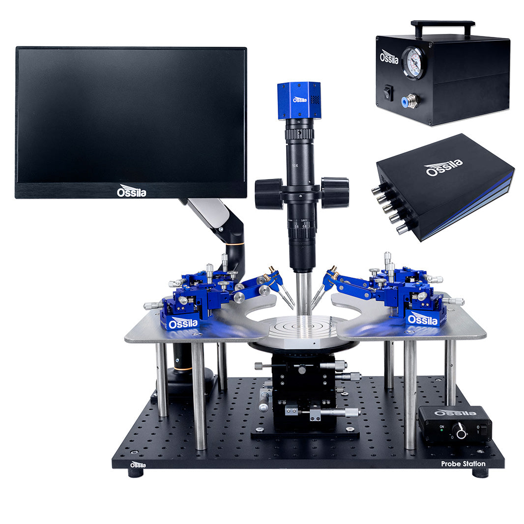
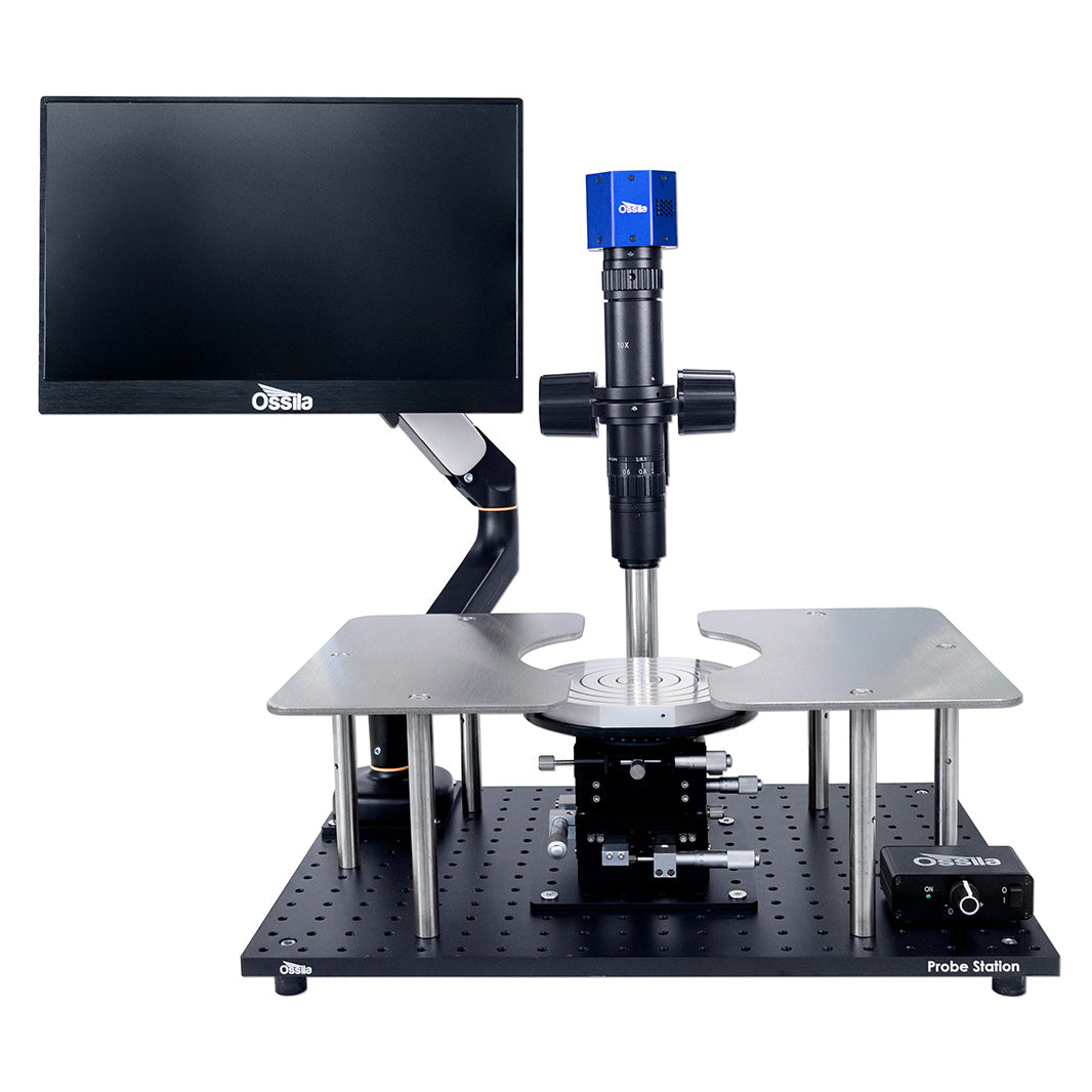
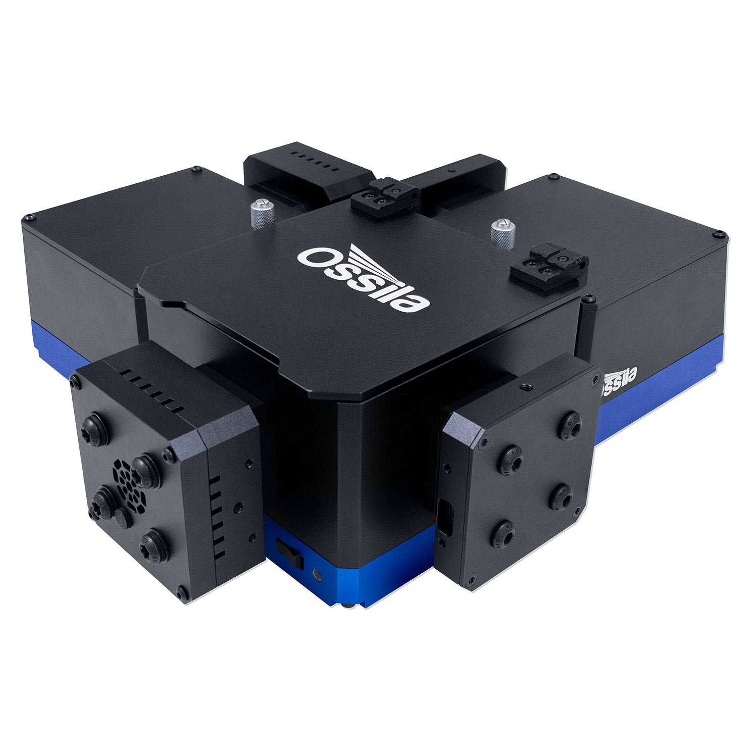
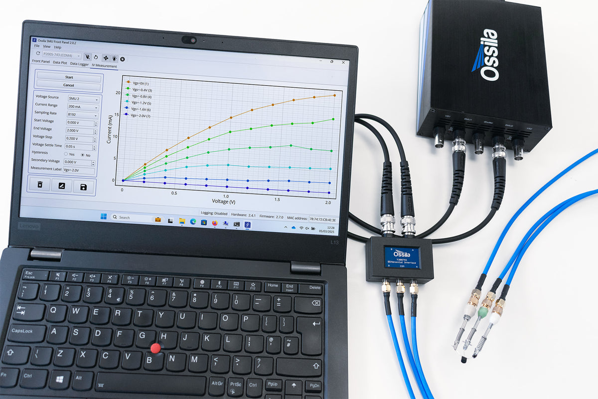
Whether you are improving existing technology or developing new devices, performing accurate device characterization is vital. These measurements can help determine device efficiency or identify issues within a semiconductor device, also referred to as the device under test (DUT). Systems like the Ossila Electrical Characterization System provide all the tools needed for these measurements, including SMU, probe station and interfaces and cables needed to connect them.
Current-Voltage (I-V) Curves
I–V curves are an important measurement in semiconductor characterization. Many semiconductor devices function as diodes, allowing current to flow in only one direction (such as in solar cell), or as transistors, which are three-terminal devices where the current between two terminals is controlled by a third (like MOSFETs).

A typical I-V curve showing diode-like behavior is shown here. The shape and scale of this curve will depend on the DUT itself e.g. the type of semiconductor, the surrounding layers and contacts and the device design.
But the performance of some semiconductor devices will depend on external factors, such as:
- Light
- External electric fields
- Temperature
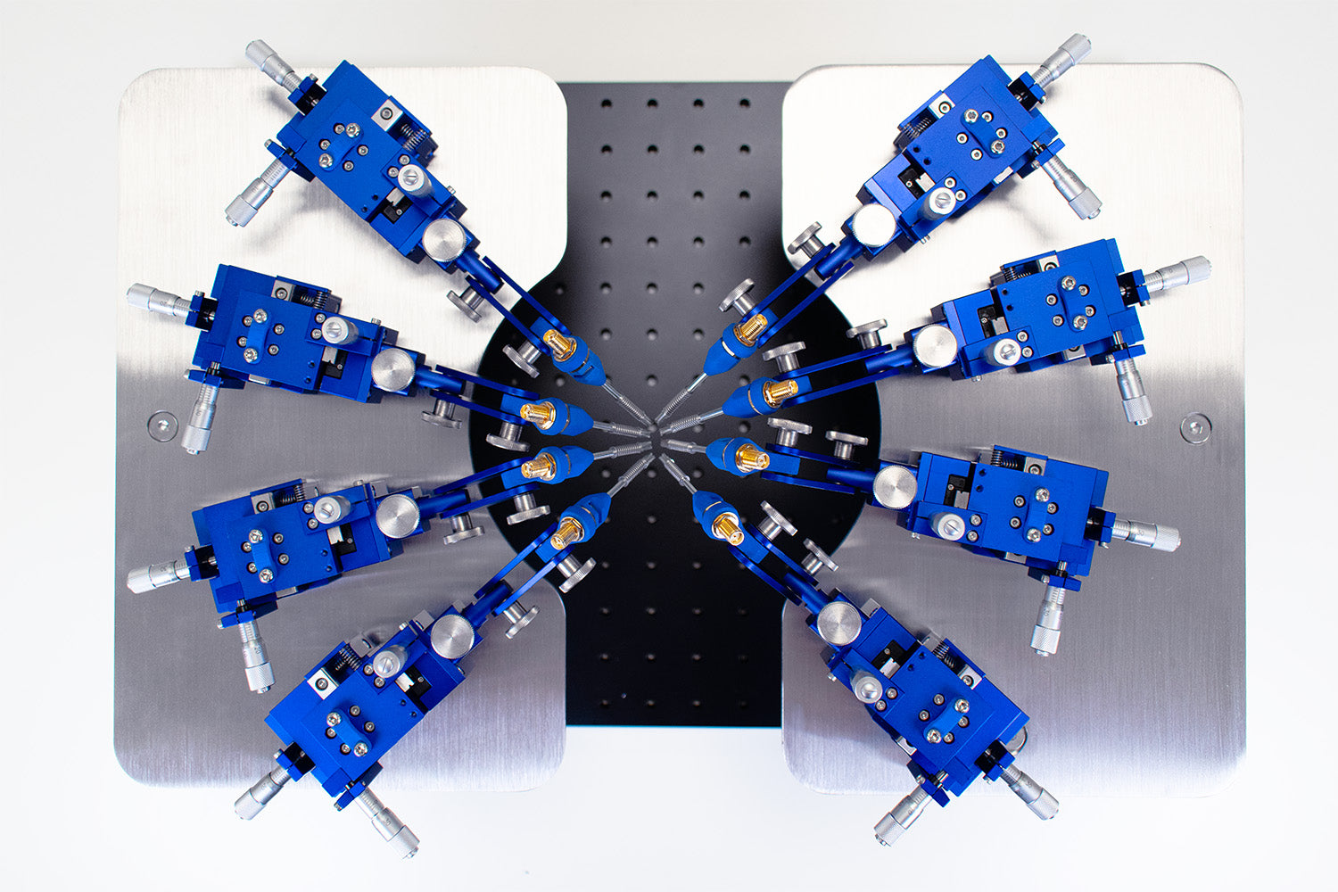
I-V curves are usually measured with a source measure unit, which varies voltage while simultaneously measuring current. Contact with the device can be made using a suitable test board, or using micromanipulators as part of a probe station.
One of the most important applications of semiconductors is transistors. The bipolar junction transistor (BJT) was very important in early semiconductor development. By measuring the collector current when varying voltage between the base and collector, you can measure key metrics such as current gain, saturation current, breakdown voltage and Early voltage. I-V curves also reveal key regions of transistor operation: cut-off, active, and saturation.
The other type of transistor device is the field effect transistor. FETs such as metal-oxide-semiconductor field-effect transistors (MOSFETs), form the basis for most modern semiconductor technology. Like a BJT, a MOSFET I-V curve can be separated into different sections: the linear and saturation regions. When measuring a field effect transistor, you vary or sweep the voltage between the drain and source (VDS), while holding the gate voltage (Vgs). By measuring several I-VDS curves at different VGS, you can measure the drain characteristics. You can also measure drain current while sweeping Vgs to get the transfer characteristics including the threshold voltage.
Another type of transistor is a Junction-Gate Field-Effect Transistor (JFET). JFETs have a direct connection between the gate and the channel, formed by the p-n junction. Key parameters that define a JFET’s behavior include the pinch-off voltage (VP), the zero-gate-voltage drain current (IDSS), and the transconductance (gm).
Organic FETs and organic thin film transistors are interesting because they have good potential for biological applications and chemical applications. In OFET biosensors, the interaction of biological molecules with an organic semiconductor will change the threshold voltage or charge carrier mobility. Both effects can be seen in the I-V sweeps. By measuring the electrical signal of the OFET you can measure molecular concentration.
For solar cells, I-V curves are crucial measurements for determining solar cell efficiency. Solar cells use semiconductors to absorb light energy and convert this into usable electrical current. In practice, the equivalent circuit for this system is an ideal current generator in parallel with a reverse diode. From a solar cell I-V curve, you can measure the open circuit voltage, short circuit current, fill factor and ultimately device efficiency. From this curve, you can also measure series resistance, shunt resistance and the maximum power point.

From I-V curves, you can also learn about general semiconductor device properties. You can investigate series resistance between layers in your device, or at the contact points. You can also probe defects or shorts in your device by examining shunt resistance. If there is a big enough shunt in your device, the I-V curve will have the straight line profile of a resistor.
Capacitance-Voltage (C-V) Measurements
Another important electrical characterization method is capacitance-voltage measurements. These can be used to test III-V compound semiconductors, MEMS and MOSFETs.
This measurement requires a capacitance meter, to sweep through different voltages while measuring capacitance. These measurements use both a DC signal and a small AC signal. The AC voltage is kept constant, while the DC voltage is swept, and capacitance across a device is measured.
C-V measurements can be useful for studying various properties of semiconductor devices such as interface traps, deep impurity levels, threshold voltages, Schottky diode barrier height and flat band voltage. On a C-V plot, the point where C=0 is equal to the Schottky barrier potential.
Characterizing Light Emitting Devices and Lasers
Light emitting diodes emit light through electroluminescence, i.e. under a bias. Therefore in order to characterize a new LED device, such as an OLED or QLED, you need to thoroughly characterize both its electrical and optical properties, often simultaneously.
Most measurements require a measurement of luminance using some sort of detector (photodetector, luminance meter, photometer) while the device is held at voltage often using a source measure unit. Examples of measurements used to measure LEDs include :
- Current efficiency: The ratio of luminous intensity to current density.
- Power conversion efficiency: The optical power output divided by electrical power in.
- External Quantum Efficiency: The quantum yield of electroluminescent devices.
- Current-Voltage-Luminance: I-V curves are plotted next to or on top of I-L curves to give a qualitative picture of an LED.
- Luminous efficiency : Luminous flux divided by electrical input power.
Like transistors, an LED's I-V curve can help you to measure the threshold voltage or "turn on" voltage.
Combinations of optical and electronic measurement techniques are used to characterize semiconductor lasers. Lasers can be optically or (most often) electrically pumped in order to create stimulated emission. For evaluating laser efficiency, output power is typically measured as a function of drive current to determine parameters such as slope efficiency and threshold current.
Testing Semiconductor Wafers and Semiconductor Metrology
Often when people refer to semiconductors, they are talking about semiconductor wafers or semiconductor chips. In industry, semiconductor devices are fabricated on silicon wafers. These wafers can be up to 300 mm in diameter and contain many individual integrated circuits or devices. Each individual device is known as a die or a chip.

Semiconductor manufacturers need to test individual dies on-wafer, firstly for quality control, and secondly to find and identify any failures. You can use micromanipulators or manual wafer probers to test individual dies. In industry, this wafer testing is usually automated, using a wafer prober and probe cards containing hundreds of tiny probes. With this system, you can test many dies on a wafer quickly and easily. For many on-wafer devices, you need to be able to achieve nm level positioning and resolution for accurate measurement.
On-wafer testing is also an important consideration for researchers. It is one thing to grow or deposit a semiconductor on a small area substrate, maintaining uniformity and high quality. However, it is a different challenge to deposit materials uniformly over a larger area. Therefore, even proof-of-concept wafer deposition and testing is beneficial to demonstrate the scalability of developing semiconductor technology. For these systems, manual probe stations are appropriate.
Wafer characterization techniques can include visual inspections to identify surface defects such as scratches, cracks, or contamination. Imaging techniques like SEM, AFM, or even visual testing under a microscope can be used to check semiconductor quality. For electrical assessments, probe stations combine with source measure units can be used to measure basic parameters like resistance, capacitance, and leakage currents across individual dies.
For high volume chip manufacturing, specialized metrology systems are designed to characterize devices inline. During large scale manufacturing, inline wafer characterization is integrated throughout the fabrication process to monitor yield-impacting variables. Semiconductor fabs routinely measure resistivity using four-point probe systems and map defects via high-resolution optical inspection or electron microscopy. Time-resolved photoluminescence or Raman spectroscopy may also be used to assess carrier lifetimes and stress states, particularly in advanced node or compound material wafers. Techniques such as Total Reflection X-ray Fluorescence (TXRF) and Vapor Phase Decomposition Inductively Coupled Plasma Mass Spectrometry (VPD-ICP-MS) are employed to detect trace metal contaminants and assess chemical purity. Additionally, electrical tests like Wafer Acceptance Tests (WAT) evaluate parameters such as threshold voltage and leakage currents to ensure device functionality.
Learn More
 What are Organic Semiconductors?
Organic semiconductors are materials, ranging from small molecules to polymers, that can transport charge. Unlike in conductors, where electrons move freely across the material, organic semiconductors rely on a structure primarily composed of carbon and hydrogen atoms.
Read more... What is a Metal Oxide Semiconductor?
Metal oxide semiconductors are comprised of positive metallic ions connected to negative oxygen ions via ionic bonds. Typically in solid form, they are non-stoichiometric compounds, which means their chemical formula cannot be exactly represented by a ratio of small natural numbers.
Learn more...
References
- Physics of Semiconductor Devices, S.M. Sze, John Wiley & Sons (1981)
- Raman spectroscopy as an advanced structural nanoprobe for..., S. Wood et al., Journal of Physics D: Applied Physics (2017)
- Stress measurements in silicon devices through Raman spectroscopy:..., I. De Wolf eyt al., Journal of Applied Physics (1996)
- Review of recent advances and sensing mechanisms in..., Benjamin King and Benoît H. Lessard, Journal of Material Chemistry C (2024)
- Expanding the potential of biosensors: a review on..., Y. Niu et al, IOP Pubishing: Material Futures (2023)
Contributors
Written by
Application Scientist
Diagrams by
Graphic Designer