Setting Up A Solar Cell Research Lab


To establish a solar cell research lab, you have to consider two main stages. You will need equipment and supplies for both:
In terms of fabrication, you must decide on the coating or deposition methods you will use. The two main approaches are thin film deposition methods, such as thermal evaporation, sputter coating or e-beam coating, and solution processing methods such as spin coating, slot die coating, spray coating, etc. You will likely need to use both approaches at some point, so access to both of these in some form would be ideal.
The ideal coating technique will depend on your coating material, other layers in your device and ultimately on the type of solar cell you want to make. Third and fourth generation solar cells, like perovskites, quantum dot solar cells and organic solar cells are quite compatible with solution processing. However, second generation inorganic solar cells, such as GaAs, are produced using evaporation methods.
You will also need to consider how you are going to accurately test your device. You need to choose a calibrated light source and an appropriate testing system. When choosing these, you need to consider device design and the size of your devices.
PV Research Lab Equipment List
Must Have
- Microbalance
- Spin Coater
- Hot plate
- Solar Simulator
- Thermal evaporator or e-beam (or access to a lab with one)
- Source Measure Unit
- Electrical Test Board
Useful to Have
- Other scalable coaters (e.g. Slot Die Coater, Doctor Blade Coater)
- UV Ozone Cleaner
- Glove Box
- Laminar Flow Hood
- Indoor Light Filter for Solar Simulator (if testing indoor PV)
Consumables Needed
- Substrates
- Micropipettes
- Measurement Aperture Mask
- Glass vials
- Annealing and Cleaning Beaker
- Deposition masks for evaporation processes
Solar Cell Fabrication
Sample Preparation
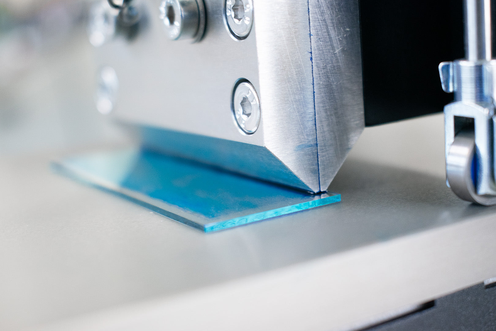
Firstly, for any thin film solar cell you will need to prepare and clean your substrates. You can clean them using simple solution based methods, i.e. sonication in DI water, Hellmanex and other solvents (acetone, IPA, etc). However, for best results, we'd recommend using a further step to remove dirt or organic matter from your substrates, such as the Ossila UV Ozone Cleaner. You will also need a microbalance for preparing coating solutions.
Coating Methods
Next, you need to choose coating equipment. The ideal deposition technique will vary from device to device, even from layer to layer. However, all solution processing techniques have different optimization parameters and methods to help you achieve uniform films. There are several solution processing machines you could choose between.
| Advantages | Limitations | |
|---|---|---|
| Spin Coater | Easiest method to optimize | Not scalable |
| Slot Die Coater | Large area coating compatible, High level of control over deposition, Very scalable technique | More complex optimization process |
| Dip Coater | Simple technique, Large area coating | Less control over deposition processes, needs large solution reservoir |
| Automatic Film Applicator | Easy large area coating, More control than dip coating, enables blade coating and bar coating | Not suitable for very thin films |
| Spray Coater | Coat over curved or irregular substrates, Scalable technique | Less control over deposition than other methods |
Environmental Control
Many perovskite and organic materials require inert processing, or at the very least controlled humidity levels, due to oxygen and moisture sensitivities. For best results, you will likely need to maintain some level of environment control. Some options for environmental control include:
- Glove Box - Creates an inert environment with low amounts of oxygen and moisture.
- Laminar Flow Hood - Reduces the amount of dust and contaminants that can affect device performance. Will not control oxygen or humidity levels.
- Dry box - An environment containing desiccants reduces levels of humidity.
Solar Cell Testing Lab
To test photovoltaic devices, you will need a calibrated light source that meets the appropriate testing standards. There are several standards, including the IEC TS 62607-7-2:2023, that are used to classify light sources. Every solar simulator is graded to one of these standards over a given area. For example, the Ossila Solar Simulator has a AAA classification over a 15 mm diameter, and an ACA classification over a 32 mm area.
Ossila offers the following solar simulator systems:
- Solar Simulator - Mimics AM1.5G spectrum to AAA classification (over 15 mm area). For testing traditional solar cells (small area devices only).
- Indoor Light Simulator - Mimics the spectrum of two types of indoor light for testing indoor photovoltaics. Meets ABSA standards over a 20 mm area.

To determine solar cell efficiency, you will need to perform a current voltage sweep (AKA an I-V measurement or a J-V measurement). Additionally, you may need to measure the lifetime of your devices. Example equipment that can be used to characterize your solar cells include:
- A source measure unit combined with an electrical test board. This is the most traditional I-V test system allowing for a range of electrical characterization measurements.
- The SMU can also be connected to the solar cell electrodes using micromanipulators. Testing stations can be set up on a probe station to allow testing of many device architectures.
- A Solar Cell I-V Test System, programmed to perform standard characterization measurements (e.g. I-V sweeps, life time measurements, stabilized current measurements). Automated systems can also change between pixels on a standard architecture device automatically.
Ossila offer solar cell testing bundles which provide everything you need to start characterizing solar cells.
- The Automated Solar Cell Testing Kit - This kit combines our solar simulator with a Solar Cell I-V Test unit. These are fitted into one unit with a bracket, so the head height is ready calibrated. The testing kit comes with all you need for automated device testing.
- Manual Solar Cell Testing Kit - This kit combines our free standing solar simulator with a source measure unit and one of our testing boards. This system is more flexible than the automated set. You can vary the head height and easily switch out the testing board.
Other Characterization Equipment
As well as J-V curve measurements, other measurements can be used to identify device issues or assess film quality.
- USB Spectrometer - for measuring transmission and absorbance properties of different device layers.
- Contact Angle Goniometer - for determining how well a layer will coat onto a substrate or neighbouring device layer.
- Four Point Probe - for assessing layer conductivity.
Learn More
 Solar Cell J-V Curve : How To Measure IV Curve of A Solar Cell
When it comes to testing the performance of solar cells, accurate measurements and reliable equipment are essential. The fundamental way to test your solar cell performance is by taking a current-voltage (I-V or J-V) measurement. The I-V curve provides valuable insights into a solar cell's efficiency, power output, and more generally electrical characteristics within the device. If you are conducting research into PV materials, understanding how to measure and interpret J-V curves is crucial in assessing device performance – but also for troubleshooting potential issues within your devices. In this article, we will guide you through the steps required to measure I-V (J-V) curves using various Ossila testing equipment.
Read more... Thin Film Deposition: Comparing Coating Methods
Thin films can be created through a range of coating methods including evaporation techniques and solution processing methods. Solution processing techniques uniformly coat a substrate with a solution, which then dries to make a thin film. Uniform and reliable thin film deposition is essential for the development and manufacture of solar cells and organic light emitting diodes, or other semiconductor devices.
Read more...