2D Materials: An Introduction to Two-Dimensional Materials

The foundation of technology is the understanding of material systems. Specific material properties are required depending on the application. For example, the electrical conductivity of copper is exploited to build circuits, the compressive strength of concrete is needed to create skyscrapers, and the durability and pliability of vulcanised rubber is important for car tyres. The more we understand about the properties of a material, the further we can push technology.
Materials at the Nanoscale
When we think about the properties of a material, we often think that they are based solely on what the material is made of. Metal conducts electricity because its atoms are held together with metallic bonds - which leave electrons free to drift through the material when an electric field is applied. Concrete is strong because it contains cement that rigidly locks incompressible pieces of sand and gravel together. Vulcanised rubber is pliable, but still durable, because it is made of flexible polymer chains that are firmly linked together.

|

|

|
However, there is something else that can affect how a material behaves: its size. This is especially true of some materials when their dimensions are reduced to the nanoscale (i.e. their size can reasonably be expressed in nanometers - generally smaller than a few hundred nanometers and down to less than a nanometer). Electrical conductivity, chemical reactivity, mechanical properties, and even how a material interacts with light can all change at the nanoscale.
As our ability to create and study nanomaterials has progressed, fascinating and unexpected new properties are being discovered. This has opened up completely new avenues for future technologies that rely on the size of a material as well as its bulk properties. We are truly entering the age of nanotechnology.
What are 2D Materials?
Nanomaterials can be broadly classified by the total number of their nanoscopic dimensions:
- If all three dimensions of a material are nano-sized, it would be called a 0D (zero-dimensional) material, more commonly known as a nanoparticle.
- If two dimensions of a material are nano-sized, with the other dimension much larger (much like a piece of string shrunk down to a tiny size), then this is a 1D material or ‘nanotube/nanowire’.
- If only one dimension is nano-sized, it would be a 2D material – resembling a large, but very thin sheet (like a piece of paper).
- Finally, if a material does not have any dimensions that are small enough to be considered nano-sized, then it is not a nanomaterial. Instead, it should be referred to as a ‘bulk’ material, and it is this class that we deal with in our everyday lives.
The table below gives a simplified explanation.
| Number of Nanoscopic Dimensions | Classification | Example |
| 0 | Bulk | Anything you can see by eye |
| 1 | 2D (nanosheet) | Graphene |
| 2 | 1D (nanotube or nanowire) | Carbon nanotube |
| 3 | 0D (nanoparticle) | Quantum dot |
With 2D materials, it is often possible to reduce the thickness of the material down to a single atom. This is the case for the most well-known 2D material - graphene - and is where the most interesting changes in properties occur.

|

|

|
Examples of 2D Materials
Graphene was the first ‘modern’ 2D material to be isolated in 2004 [1]. Since then, there have been literally hundreds of other examples [2] along with other graphene materials, with an extensive range of properties. Below are several that are being actively researched.
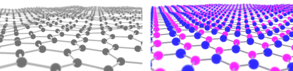
Graphene and hexagonal boron nitride
Graphene is a covalently-bonded hexagonal lattice of carbon atoms just one atom thick (about 0.14 nm). It is a semimetal (its conduction and valence bands both touch). Graphene's unique band structure means that electrons move through it at extremely high speeds (about 1/300 the speed of light), giving it fascinating properties - such as unparalleled thermal conductivity.
Optically transparent, graphene absorbs only 2% of incident visible light and has the highest tensile strength of any material. A single monolayer of graphene, just 0.3 nm thick, would be able to support the weight of a football [3].
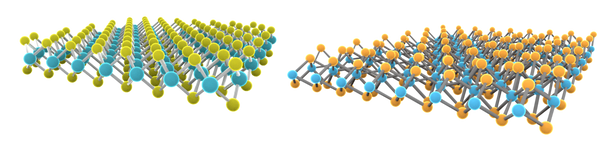
Transition Metal Dichalcogenides (TMDCs)
Transition metal dichalcogenides (commonly referred to as TMDCs) have the chemical formula MX2, where M is a transition metal (such as molybdenum (Mo) or tungsten (W)) and X is a chalcogen (such as sulfur (S), selenium (Se) or Tellurium (Te)). Bulk TMDCs are van der Waals materials with each layer being three atoms thick, consisting of the metal layer sandwiched between two chalcogenide layers.
TDMCs can take various crystal structures. The most common is the 2H-phase with trigonal symmetry, which results in semiconducting characteristics such as possessed by MoS2, WS2, MoSe2. These semiconductors have an indirect bandgap when in the bulk. For monolayers, the bandgap becomes direct and in the visible spectrum, making them attractive for optoelectronics. Charge mobilities of ~100-1000 cm2V-1s-1 make them a popular choice for 2D transistors. Another possible structure is the metallic 1T phase, which is the most stable polymorph of WTe2.
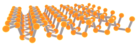
Phosphorene
Phosphorene is a single layer of black phosphorus – a layered, stable allotrope of elemental phosphorus. It is a direct bandgap semiconductor with a puckered honeycomb structure. The bandgap can be tuned throughout the visible region by stacking layers on top of each other. It has good charge mobility (~1000 cm2V-1s-1), therefore making it suitable for optoelectronic devices and transistors. Phosphorene's corrugated structure means that its properties can vary significantly, depending on which direction the material is measured along.
Xenes
Monolayers of silicon (silicene), germanium (germanene) and tin (stanene), are collectively known as Xenes (following the naming convention of graphene). They have a hexagonal structure similar to graphene, but are buckled to varying degrees. Unlike graphene, they cannot be exfoliated from bulk material and must be epitaxially grown on a substrate, and generally retain a strong interaction with that substrate. While still very much in their infancy, potential applications range from field-effect transistors to topological insulators.
Recently, 2D analogs of antimony [4] and bismuth [5] (antimomene and bismuthine respectively) have also been grown. Bismuth shows potential for magneto-electronic applications [6].
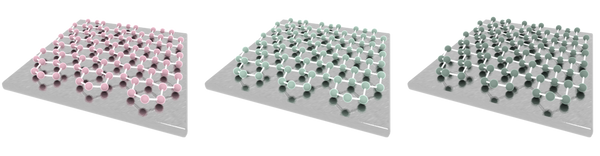
Examples of Popular 2D Materials
The 2D material families mentioned above are available for purchase in their 3D bulk crystal or powder form, which can be easily exfoliated into 2D layers. Some materials are also available directly in their 2D form, either as nanoplatelets or as thin films on various substrates. Feel free to contact us for advice on selecting the best 2D materials for your research. Below are a few examples of the materials we offer:


How Do We Make 2D Materials?
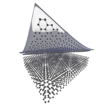
It is possible to take any material and thin it down (until it has a thickness of only a few atoms) to create a 2D material. However, many materials (e.g. diamonds) have chemical bonds oriented in 3-dimensions, so thinning the material requires cutting these bonds – leaving them ‘dangling’. A 2D material created in this way will have a high density of dangling bonds, which are chemically and energetically unstable, and can force the material to rearrange its structure to lower its surface energy.
Another allotrope of carbon – graphite – has strong chemical bonds only along planes within the bulk material. These planes are stacked on top of each other and held together by weak van der Waals interaction, and so can be separated without leaving any dangling bonds. In the case of graphite, a single plane is called graphene. Most of the 2D materials being studied therefore belong to the broader class of layered materials (or van der Waals materials).
There are two methods for making 2D materials:
i) Top-down (start with a bulk material and make it thinner)
ii) Bottom-up (start with the atomic ingredients and assemble them together)
Within each of these approaches are several subcategories, each with their own advantages and disadvantages - explained below.
Top-down
Mechanical exfoliation
Commonly known as the ‘Scotch-tape method’, it was first used to create monolayer graphene. A piece of sticky tape is applied to the surface of a layered material and then peeled off, taking flakes (consisting of a small number of layers) with it. The tape can then be pressed onto a substrate to transfer the flakes for study. The monolayer yield of this process is low (the flakes obtained are mostly multilayer), with no control over the size and shape. However, the size of monolayer flakes that can be produced is reasonable (from a few microns up to ~100 microns) and the quality of monolayers is excellent - with very few defects due to the lack of chemical processing involved. To reduce the risk of contamination and increase the quality of the monolayers, this process can also be carried out inside a glove box.
It is also a suitable technique for all van der Waals materials. For these reasons, mechanical exfoliation remains popular for lab-based studies, but it is not scalable for integration into new technologies.
Mechanical Exfoliation Video Guide
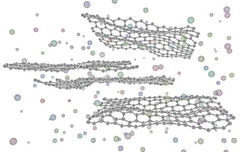
Liquid exfoliation
Another mechanical method, liquid exfoliation involves using an organic solvent as a medium to transfer mechanical force to the layered material (often in the form of a powder) suspended in the liquid. Sonication causes tensile stress to be applied to the layers, forcing them apart. To improve monolayer yield, variations exist - such as introducing reactive ions (between the material layers that create hydrogen bubbles) that push the layers apart, or that rapidly mix the solution to create additional shear force on the layers.
This method is highly scalable but has several drawbacks. The monolayer yield is again generally low, and the flakes are often less than 100 nm in size (due to the applied forces breaking them apart). The resultant flakes may also potentially have a high density of defects and residual solvent when removed from solution, making them unsuitable for many optoelectronic applications.
Bottom-up
Chemical vapor deposition
This process involves passing one or more precursor gases (which usually contain the atomic ingredients of the required film) through a heated furnace, where they will react together or with a substrate and form a thin layer of the required material. This process has been successfully applied to grow graphene and TMDCs. Several parameters (such as gas pressures and compositions, temperature, and reaction times) need to be controlled as they will affect the thickness, quality and composition of the films. While this process is more complex and expensive than most top-down techniques, it is highly scalable, and the quality of the films produced approaches that of mechanically-exfoliated layers.
Solution-based chemical synthesis
A vast variety of techniques have been developed to synthesize 2D materials through wet chemical techniques. These include high-temperature chemical reactions in solution, interface-mediated growth (reactions occur only at the surface of a liquid), fusion of nanoparticles into larger nanosheets, and many more. Each method is particularly well-suited to a certain type of 2D material, and everything from graphene and TMDCs to monolayer metals can be synthesized using the appropriate technique.
The lateral size of the flakes produced by these methods is generally small (<100’s nm), and the techniques share the same residual solvent problem as liquid exfoliation. However, for certain applications, the scalability, low cost and versatility of these techniques makes chemical synthesis the best method for large-scale production.
Why are 2D Materials Different from Bulk Materials?
This comes down to three reasons:
-
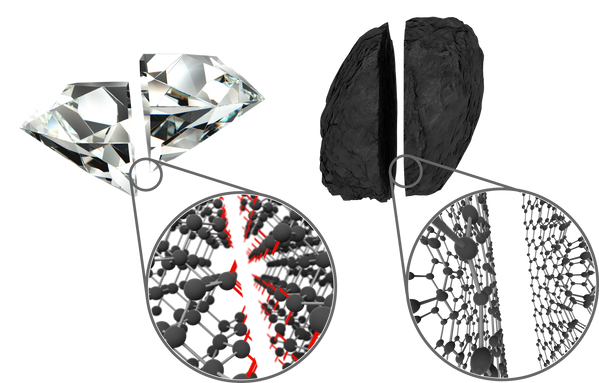
Removal of van der Waals interactions – A layered bulk material consists of many covalently-bonded planes held together by weak van der Waals interactions. When a force is applied to a material, these van der Waals forces can be easily overcome and the material breaks – making it seem weak. Conversely, the covalent bonds that hold the atoms together in the layers are actually very strong. A monolayer will only have covalent bonds. By removing the ‘weak links’ from the material, it appears to become much stronger. For example, graphene has a tensile strength 1000 times greater than graphite, and while a graphite pencil can be easily broken, graphene is over 100 times stronger than steel.

Graphite (left) can be easily broken because of its weak interplane van der Waals forces, while graphene (right) has only covalent bonds and so it extremely strong - a monolayer is strong enough to support a football.
-
An increase in the ratio of surface area-to-volume – The surface area-to-volume ratio of a material defines how much of it is exposed to its environment. This is important for chemical reactions – the more reactant that is in contact with the material, the faster the reaction can occur, so 2D materials tend to be more reactive their bulk counterparts. It also makes 2D materials more sensitive to their surroundings, an effect that is exploited for sensors based on 2D materials.

When an object is divided into smaller components, its total surface area increases. From left to right: a bulk object is divided into 2D sheets - exposing the red surfaces, and the sheets are divided into 1D rods - further exposing the blue surfaces. Finally, the rods are divided into dots - exposing additional green surfaces.
-
Confinement of electrons in a plane – The electronic and optical properties of a material depend upon its electronic band structure. This describes how electrons move through the material, and is a result of the periodicity of its crystal structure. When a material goes from bulk to 2D, the periodicity is removed in the direction perpendicular to the plane, which can greatly change the band structure. The modified band structures are responsible for the extremely high conductivity of graphene and the fluorescence of monolayer MoS2.

Band structure diagram of (left) bulk and (right) monolayer MoS2 showing the crossover from indirect to direct bandgap accompanied by a widening of the bandgap. Another effect of dimensional confinement is reduced dielectric screening between electrons and holes in semiconductors. When there is less material to screen the electric field, there will be an increase in Coulomb interaction and more strongly-bound excitons – making them more stable than excitons found in bulk materials. If the excitons are confined in a plane that is thinner than their Bohr radius (as is the case for many 2D semiconductors), quantum confinement will result in an increase in their energy compared to bulk excitons, changing the wavelength of light they absorb and emit.
Their energy can be tuned somewhat by changing the number of layers in the 2D material (i.e. a bilayer structure will absorb/emit lower energy light than a monolayer). However, this can also affect the band structure, resulting in changes to other properties as well (for example, bilayer MoS2 becomes non-emissive compared to a monolayer due to changes in electronic band structure).
2D Materials

Applications of 2D Materials
The change in properties, caused by a reduction in the dimensionality of 2D materials, means that they are often well-suited to applications where the bulk material would be unsuitable. Below is a list of some of the most promising applications.
Transistors and sensors
Field-effect transistors (FETs) have been fabricated from a variety of semiconducting 2D materials such as TMDCs [7] and black phosphorus [8]. Their good charge mobility and moderate bandgaps make them good candidates for this application.
Hexagonal boron nitride is often used as the gate dielectric. Despite its intrinsic lack of bandgap, graphene has also been used as the active channel in transistors by opening up a bandgap with methods such as engineering edge states, chemical doping, or applying electric fields.
An advantage of 2D materials over conventional silicon is their inherent flexibility. In combination with suitable substrates, 2D materials can be used to create flexible circuits [9]. While there are still some issues with large-scale production of high-quality 2D layers that would be required by the electronics industry, transistors remain one of the most promising applications. FET-based sensors have been fabricated from 2D TMDCs that can detect a range of chemicals in the parts-per-million range or better, including triethylamine [10], nitric oxide [11], ammonia, and nitrogen dioxide [12] by measuring changes in conductance when exposed to these chemicals.
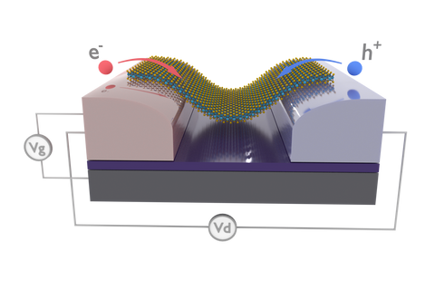
Photodetectors
Many TMDCs (e.g. MoS2, MoSe2, WS2 and WSe2) and black phosphorus have a bandgap in the optical or near infrared region and good charge transport characteristics. A single monolayer of TMDC (< 1nm thick) can absorb up to 10% of incident visible light [13], equivalent to approximately 100nm of silicon. Due to the thinness of the monolayers, this absorption is not enough for high efficiency photovoltaics. However, they can be fabricated into high efficiency photodetectors. A device fabricated from a mechanically exfoliated MoS2 monolayer achieved a sensitivity of ~103 A/W over the spectral range 400nm-680nm [14], while combining MoS2 with graphene into a heterostructure the sensitivity reached 108 [15].
Battery electrodes
Electrodes for ion batteries and supercapacitors require electrically conductive materials with a high surface area to store high densities of ions. Graphene has received some attention as a possible successor to graphite electrodes [16, 17] due to its higher surface-to-mass ratio, higher conductivity, greater mechanical strength, and flexibility [18] which could lead to stronger, lighter batteries with greater power densities and faster charging times. 2D MoS2 has also received a lot of attention as a possible electrode. While it is semiconducting in its most stable 2H crystal structure, it can be prepared in such a way (usually by chemical exfoliation) such that it adopts a metallic 1T phase. Electrodes formed from stacked 1T monolayers have shown higher power and energy densities than graphene-based electrodes [19].
Topological insulators
Topological insulators (TIs) are materials that behave as insulators, except for at their edges where they can conduct electrons with high efficiency. Electrons with opposite spins travel around the edges in opposite directions. TIs may find practical applications in low-power electronic and spintronic devices (where electron spin is used to encode information or improve device performance). The Xenes (in particular bismuthene and stanine) are expected to act as TIs [20]. The TMDC WTe2 can be switched between topological insulator and superconductor with an electric field [21, 22].
Valleytronics
Valleytronics utilizes a property of charge carriers in some TDMCs (e.g. MoS2, WS2) called 'valley polarization'. This property is linked to the spin and angular momentum of the electron and hole. Polarized optical excitation allows selective excitation of a particular valley, and hence carriers of a specific spin. This additional degree of freedom opens up the potential to create novel optoelectronic devices for data processing and storage.
Learn More
 Graphene Properties and Applications
Graphene materials have ultrahigh surface area, high strength, and exceptional conductivity making them highly valuable for various applications. Its large surface area enhances energy storage, sensor sensitivity, and water purification efficiency. Graphene's incredible strength and lightweight nature are ideal for flexible electronics and mechanical reinforcement. Additionally, its excellent electrical and thermal conductivity support advanced electronic devices, energy storage systems, and efficient heat management.
Read more... What is a Photodetector?
A photodetector is a device that can detect light, or more specifically photons. They are classed as optoelectronic devices like photovoltaic devices. This is because they produce an electronic signal which is proportional to the incident optical input.
Read more...References
- Electric Field Effect in Atomically Thin Carbon Films, KS. Novoselov et al., Science, 306, 666-669 (2004)
- Two-dimensional materials from high-throughput computational exfoliation of experimentally known compounds, N. Mounet et al., Nature Nanotechnology, 13, 246-252 (2018)
- Measurement of the Elastic Properties and Intrinsic Strength of Monolayer Graphene, C. Lee et al., Science, 321, 385-388 (2008)