Probe Station

Buy a probe station | SMU connectors & cables | Parts & accessories | Key components | Applications | Resources & support
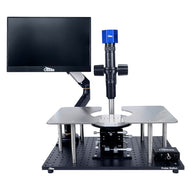
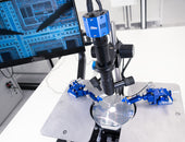
Reject the inflated costs of overengineered systems with a probe station that delivers exactly what you need for high-performance, micron-scale probing at a fair price. When set up as the electrical characterization system, you have everything you need to reliably probe, test, and characterize the electrical properties of semiconductor wafers and small-scale electronics.
Ossila probe stations are built to accommodate customization so you can configure a setup that works specifically for you, with Ossila micromanipulators and a suite of electrical characterization tools. The practical and intelligent design of each component means you can prioritize your research instead of being limited by unnecessary complexity.
Set up a probe station


Connectors and cables


Probing parts and accessories


Key components of a probe station
To create the specialized system that helps to conduct precise electrical measurements on small devices or sensitive materials, Ossila probe stations combine essential and useful components. Built into one system, they work with measurement instruments to analyze electrical parameters, enabling highly accurate testing.

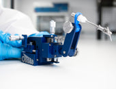
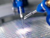
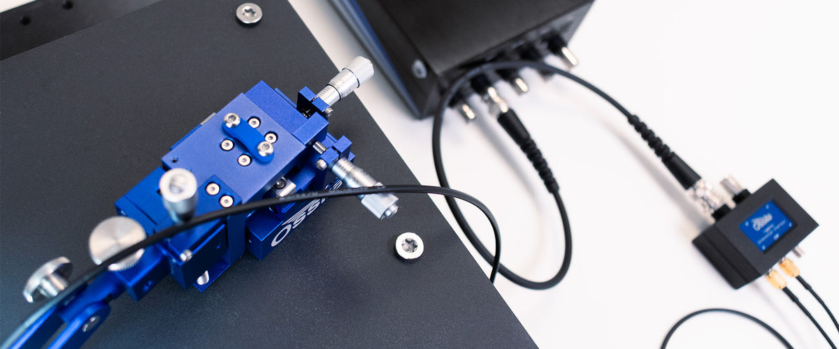
Micromanipulators
Ossila manual micromanipulators are used to precisely position probe needles on tiny contact points of a sample, with micron-level accuracy. The direct, hands-on control is intuitive, straightforward, and low cost. With excellent tactile feedback and minimal backlash or drift, you can make intuitive probe adjustments down to2 μm along three axes. The magnetic base and compact size integrate seamlessly into our probe station, making it comfortable to use multiple micromanipulators along side each other.
Probes Tips and Attachments
Fine-tipped probes are essential to making precise contact with the device under test. Choose from high-purity tungsten or BeCu with 20 µm or
5 µm tip diameters to suit your specific probing and experimental requirements. Where probing is not your sole focus, a universal tool clamp expands the potential of your micromanipulator. Position a range of additional tools from 1 mm to 13 mm in diameter such as syringes, optical fibers, and vacuum needles.
In-Built Vibration Isolation
Designed with elastomeric vibration dampening mounts to stabilize probe contact, our probe station base is capable of isolating any frequencies above 17 Hz. Electrical measurements involving very small contact points, low currents, or high frequencies are extremely sensitive to mechanical vibrations. The effective isolation prevents external vibrations from lab equipment, foot traffic, or building HVAC systems from causing probe tips to skate across contact pads or damage delicate samples and probes.
Optical Microscope
The digital microscope delivers lag-free feedback in your probing and positioning processes to simplify and streamline your workflow. Integrated into Ossial probe stations, the long working distance provides ample space between the lens and sample to work comfortably. ability to capture images during probing. With simultaneous HDMI and USB 3.0 outputs, view a live image while capturing high-resolution images and video on your computer for analysis and documentation.
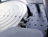
Wafer Chuck
A stable platform for your sample or device under test is essential for consistent probe contact and high quality, reliable measurements. Knowing your samples are secure lets your focus on your your experiment and not on the quality of the setup. Securely hold samples from 5 mm to
150 mm with 6 definable vacuum zones across the precision-engineered wafer chuck when you use the compatible vacuum pump to complete your wafer probe station.
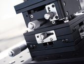
Positioning Stage
As well as our micromanipulators, the manual stage also offers direct, hands-on adjustment via micrometers. Perfect for varied adjustments to your sample position, a manual stage keeps your setup simple to use. Motion along three linear axes – X, Y (for planar movement across the sample) and Z (for vertical adjustment to make or break probe contact) – and a rotational (theta) axis for fine angular alignment of the sample make sample positioning and contact easy.
Probe station applications
Probe stations are integral in fields like semiconductor manufacturing, electronics research, telecommunications, and automotive and aerospace industries. Whether you're working with compound semiconductors, organic and flexible electronics, thin film devices, photodetectors and sensors, or emerging materials, our probe station products support a range of testing setups.
Wafer-Level Testing
Wafer probe stations are essential in fields like semiconductor manufacturing for wafer-level testing. Before a wafer is diced into individual chips, it undergoes testing to assess the performance of each die. This early-stage testing helps manufacturers identify faulty dies, reducing waste and improving overall production efficiency.

Failure Analysis
When a device malfunctions, a probe station can be used to pinpoint the root cause of the failure. By systematically probing different parts of the device, engineers can identify defective components or faulty connections. This information is crucial for improving future designs and manufacturing processes.
Research and Development (R&D)
In R&D environments, probe stations are used to test new materials, device structures, and fabrication processes. Researchers can use them to explore the electrical properties of novel materials like organic semiconductors, 2D materials, and nanostructures.
Device Characterization
Probe stations are also used to measure a wide range of electrical parameters, including DC characteristics like current-voltage (I-V) curves and capacitance-voltage (C-V) curves, as well as RF characteristics such as S-parameters. By analyzing these measurements, engineers can gain insights into the device's performance, reliability, and suitability for specific applications.
Optoelectronic Testing Stations
In addition to electrical testing, probe stations can be used to test optoelectronic devices, such as photodiodes, LEDs, and laser diodes. By integrating optical sources and detectors into the setup, engineers can measure the performance of devices that interact with light, which is crucial for applications in fiber optics, solar cells, and display technologies.
Life Sciences
These instruments are also crucial in electrophysiology, where they are used to position microelectrodes with extreme precision to record electrical activity from individual neurons or muscle cells. This allows researchers to study ion channel behavior, synaptic transmission, and neural circuitry in real-time. In cell biology, micromanipulators are used for various tasks, such as injecting biological molecules into cells, performing patch-clamp experiments, or isolating specific cells for further analysis. They are also employed in genetic engineering for microinjection of DNA or RNA into embryos or cells, and in microdissection to manipulate or dissect small tissue samples under a microscope.
Resources
About Our Equipment
 Connecting the Micromanipulator to the Source Measure Unit
This guide gives an overview of how to use the Ossila Micromanipulators with the Source Measure Unit, as well as some general tips and tricks for getting the most out of sensitive electrical probing measurements.
Read more... Micromanipulator Drift and Other Common Errors
The performance of a micromanipulator can suffer from various mechanical issues, including drift, backlash, side play, and sticking. Understand these issues and how our engineers have implemented solid design principles to avoid potential movement issues from the start.
Read more... Probe Station Features: What Do I Need?
Probe stations are incredibly useful for a wide range of experiments, from semiconductor characterization to electrophysiology. However, each experiment will have different requirements and every lab has its own demands. This raises the question: what probe station features do you need?
Read more...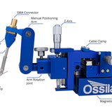 Getting the Most Out of Your Ossila Micromanipulator
This guide is designed to help you set up, connect, and tailor your Ossila Micromanipulator to your specific research needs. We believe that precision instruments should provide intuitive control, and our goal is to help you achieve that. Whether you are performing an initial setup or advanced modifications, we are here to support you.
Read more...Electronics Resources
 Contact Resistance and Lead Resistance in Probe Stations
Minimizing electrical resistance is a key consideration when selecting components for use in probe stations. Lower resistance allows current to flow more easily through the probes to the measurement device, without affecting the measurement itself. There are multiple things that can contribute to resistance in measurement devices.
Read more... Leakage Current: Definition, Examples and Leak Resistance
Leakage current refers to any unwanted current that flows outside of the desired circuit path, adding to the noise of a measurement. Leakage currents can arise from many things, such as:
Read more... Coaxial Cables and Triaxial Cables
For many electrical measurements, the cable that connects your instrument to your device is a simple wire. But when you are working at the limits of sensitivity—measuring picoamps of current, sourcing from gigaohm impedances, or capturing fleeting signals—your choice of cable becomes a critical part of your experimental setup.
Read more...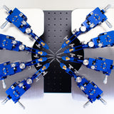 Semiconductor Characterization Methods for Materials and Devices
Semiconductor characterization refers to the process of measuring and evaluating the properties of a semiconductor. This is quite a broad term and can refer to different processes depending on the context. It can refer to:
Read more...Technical support