Leakage Current: Definition, Examples and Reduction

Leakage current refers to any unwanted current that flows outside of the desired circuit path, adding to the noise of a measurement. Leakage currents can arise from many things, such as:
- The amount of current drawn when a circuit is off, or when the current should be zero.
- Any current that flows from a live circuit into the instrumentation, into the grounded state or between conductive parts of a system that are supposed to be electrically isolated.
Leakage current is often measured in nanoamperes (nA) or picoamperes (pA).
In all cases, you want leakage current to be as low as possible. Leakage current is generally negligible in devices that draw large amounts of current. However, leakage current will have more impact on a measurement when measuring lab scale devices. This can even impact devices which draw milliamperes of current, such as OFETs or solar cell devices. In extremely low-current systems, even a few picoamperes of leakage may exceed the signal of interest, leading to inaccurate readings.
Even in traditional silicon chips, the effect of leakage currents on device performance has increased. Thanks to Moore's law, as the density of transistors on microchips increases, the impact of leakage losses also increase. Therefore, to improve microprocessor design, it is more important than ever to measure leakage current accurately.
Leakage current can distort sensitive electrical measurements by introducing offset errors and by increasing background noise. It can also compromise circuit isolation, causing unintended current paths or ground loops. This is especially critical in applications like electrophysiology, semiconductor testing, or nanodevice characterization, where precision is essential.
Examples of Leakage Current
Thin Film Silicon Devices
Leakage current can be an issue in thin film semiconductors, such as silicon-on-insulator devices. In thin films, small amounts of current leakage can drastically affect device performance. Mechanisms that increase leakage currents in thin film silicon-on-insulator devices include:
- Low threshold voltages due to inconsistent doping leading to leakage when the system should be "OFF"
- Back channel effects where current flows through a "back channel" in the device.
- Defect-induced leakage, where defects create carrier pathways, affecting carrier flow
- Inconsistencies at device edges can affect the threshold voltage and create unintended conductive paths.


Organic Thin Film Transistors
There are also many mechanisms that will increase leakage current in organic thin film transistors. These can include :
- Leakage through the gate insulator: the gate insulator is meant to keep the gate and the organic semiconductor isolated. If there is current leakage at this point, current will escape affecting device performance.
- Intrinsic leakage: Through the movement of minority charge carriers when the OTFT is in OFF state.
- Parasitic leakage (outside of the OFET channel): Including losses via the electrode contacts or through external circuit. These will be affected by the contact resistances, leakage current through probes and wires, and other external circuit-related parasitic losses.
Solar Cells
In the study of solar cells, leakage current is usually incorporated into a solar cell's shunt resistance, so will affect the fill factor and subsequently the efficiency of a solar cell.
In particular, leakage current may be an issue with indoor OPV devices or any devices which are tested under low-intensity illumination . In testing indoor PV devices, it is important that leakage current can be accurately measured. Grain boundaries can also provide an opportunity for intrinsic current leakage.
Leakage Current in Electrical Measurement Equipment
The job of measurement equipment is to accurately measure a sample property, while imposing as little on the measurement as possible. Any leakage current through measurement equipment will be lost from the measurement, making it less accurate. Therefore, any electrical characterization equipment should aim to minimize leakage current as much as possible.
Micromanipulators
Leakage current is a defining feature of probes, micromanipulators, and probe stations, as it can drastically impact the types of measurements they can perform. Some measurements require probes and systems with extremely low level of leakage current. Ideally, leakage current should be several orders of magnitude lower than the measurement you are trying to measure.

For example if you are trying to measure currents of mA, you need measurement equipment with leakage current in the nanoamperes range. However, if you are characterizing currents of picoamperes, you will need extremely specialist probes for this measurement.
The Ossila Micromanipulator has leakage currents of <100 pA at 75 V DC, so is suitable for a range of different device characterization measurements.
Micromanipulator

Testing boards
The Ossila testing boards have intelligent track design to reduce leakage currents as much as possible. Additionally, the High Density OFET test boards have specially designed pixel switches to prevent leakage when the switch is OFF, while showing negligible extra resistance when the current flow is ON.
More Resources
 Contact Resistance and Lead Resistance in Probe Stations
Minimizing electrical resistance is a key consideration when selecting components for use in probe stations. Lower resistance allows current to flow more easily through the probes to the measurement device, without affecting the measurement itself. There are multiple things that can contribute to resistance in measurement devices.
Read more...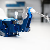 Connecting the Micromanipulator to the Source Measure Unit
This guide gives an overview of how to use the Ossila Micromanipulators with the Source Measure Unit, as well as some general tips and tricks for getting the most out of sensitive electrical probing measurements.
Read more...
References
- Leakage Current: Moore’s Law Meets Static Power, N.S. Kim et al., IEEE Computer Society (2003)
- Leakage current models of thin film silicon-on-insulator devices, H. Shin et al., Applied Physics Letters (1998)
- Eliminating Leakage Current in Thin-Film Transistor of Solution-Processed..., L. Han et al., Advanced Electronic Materials (2022)
- Different Morphology Dependence for Efficient Indoor Organic Photovoltaics:..., X. Zhou et al, Applied Materials and Interfaces (2021)