Molybdenum Disulfide (MoS2): Theory & Applications

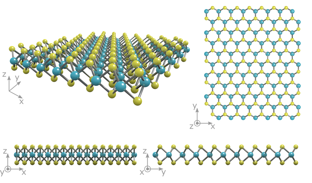
Molybdenum disulfide belongs to a class of materials called 'transition metal dichalcogenides' (TMDCs). Materials in this class have the chemical formula MX2, where M is a transition metal atom (groups 4-12 in the periodic table) and X is a chalcogen (group 16). The chemical formula of molybdenum disulfide is MoS2.
The crystal structure of molybdenum disulfide (MoS2) takes the form of a hexagonal plane of S atoms on either side of a hexagonal plane of Mo atoms. These triple planes stack on top of each other, with strong covalent bonds between the Mo and S atoms, but weak van der Waals forcing holding layers together. This allows them to be mechanically separated to form 2-dimensional sheets of MoS2.
Following on from the huge research interest in graphene, MoS2 was the next 2-dimensional material to be investigated for potential device applications [1]. Due to its direct bandgap, it has a great advantage over graphene for several applications, including optical sensors and field-effect transistors.
Properties of MoS2
Bulk properties
MoS2 occurs naturally as the mineral 'molybdenite'. In its bulk form, it appears as a dark, shiny solid. The weak interlayer interactions allow sheets to easily slide over one another, so it is often used as a lubricant. It can also be used as an alternative to graphite in high-vacuum applications, but it does have a lower maximum operating temperature than graphite. Bulk MoS2 is a semiconductor with an indirect bandgap of ~1.2eV, and is therefore of limited interest to the optoelectronics industry.
Optical and electrical properties
Individual layers of MoS2 have radically different properties compared to the bulk. Removing interlayer interactions and confining electrons into a single plane results in the formation of a direct bandgap with an increased energy of ~1.89eV (visible red). A single monolayer of MoS2 can absorb 10% of incident light with energy above the bandgap [2]. When compared to a bulk crystal, a 1000-fold increase in photoluminescence intensity is observed, but it remains relatively weak - with a photoluminescence quantum yield of about 0.4% [1]. However, this can be dramatically increased (to over 95%) by removing defects that are responsible for non-radiative recombination [3].

The bandgap can be tuned by introducing strain into the structure. A 300 meV increase in bandgap per 1% biaxial compressive strain applied to trilayer MoS2 has been observed [4]. The application of a vertical electric field has also been suggested as a method of reducing the bandgap in 2D TMDCs - potentially to zero, thereby switching the structure from semiconducting to metallic [5].
Photoluminescence spectra of MoS2 monolayers show two excitonic peaks: one at ~1.92eV (the A exciton), and the other at ~2.08eV (the B exciton). These are attributed to the valence band splitting at the K-point (in the Brillouin zone) due to spin-orbit coupling, allowing for two optically active transitions [6]. The binding energy of the excitons is >500meV. Hence, they are stable up to high temperatures.
Injecting excess electrons into MoS2 (by either electrical [7] or chemical [8] doping) can cause the formation of trions (charged excitons), which consist of two electrons and one hole. They appear as peaks in the absorption and PL spectra, red-shifted by ~40meV with respect to the A exciton peak (tunable through doping concentration). While the binding energy of trions is much lower than that of the excitons (at approximately 20meV), they have a non-negligible contribution to the optical properties of MoS2 films at room temperature.
MoS2 monolayer transistors generally display n-type behaviour, with carrier mobilities approximately 350cm2V-1s-1 (or ~500 times lower than graphene) [9]. However, when fabricated into field-effect transistors, they can display massive on/off ratios of 108, making them attractive for high-efficiency switching and logic circuits.
Mechanical properties
MoS2 monolayers are flexible, and thin-film FETs have been shown to retain their electronic properties when bent to a 0.75mm radius of curvature [10]. They have a stiffness comparable to steel, and a higher breaking strength than flexible plastics (such as polyimide(PI) and polydimethylsiloxane (PDMS) [11]), making them particularly suitable for flexible electronics.
At around 35Wm-1K-1, the thermal conductivity of MoS2 monolayers is ~100 times lower than that of graphene [12].
Valleytronics
MoS2 and other 2D TMDCs may offer a route to technologies beyond electronics, where degrees of freedom (other than charge) can be utilized for information storage and/or processing [13].The electronic band structure of MoS2 displays energy maxima of the valence band, and minima of the conduction band at both the K and K’ (often called -K) points of the Brillouin zone. These two discrete ‘valleys’ have the same energy gap but are discrete in position in momentum space.
The optical transitions in these valleys require angular momentum changes of +1 for the K-point, and -1 for the K’ point[14]. Hence, excitons can be selectively excited into a valley with circularly polarized light - with right-handed (σ+) polarized light exciting excitons in the K valley, and left-handed (σ-) polarized light exciting excitons in the K’ valley.
Conversely, light emitted from exciton recombination in the K valley will be σ+ polarized, and light emitted from exciton recombination in the K’ valley will be σ- polarized. Since these valleys can be independently addressed, they represent a degree of freedom called 'valley pseudospin' [15] that could be used in ‘valleytronic’ devices.
Furthermore, the spin-orbit split valence band at the K and K’ points has opposite signs of spin for each of the valleys [16]. For example, an A-exciton in the K valley consists of a spin-up electron and a spin-down hole, and a K valley B-exciton has a spin-down electron and spin-up hole. For A and B excitons in the K’ valley, their constituent charge carriers have the opposite spin.
| σ+ (K valley) | σ- (K’ valley) | |
| EA | ↑e ↓h | ↓e ↑h |
| EB | ↓e ↑h | ↑e ↓h |
This means that the valley pseudospin and charge carrier spin degrees of freedom are coupled (spin-valley coupling), and the spin and valley properties of charge carriers can be selected optically - through choice of excitation polarization (to choose the valley) and energy (to select the A or B exciton - and hence, the spin) [17].
When an in-plane electric field is applied, excitons may become disassociated [18], with the carriers retaining their valley and spin characteristics. Electrons (and holes) in opposing valleys will travel in opposite directions perpendicular to the field. This is called the 'valley Hall effect', and could form the basis of future technologies, where more information can be encoded onto electrons because of these added degrees of freedom.
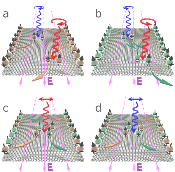
a) σ+ circularly polarized light incident on a monolayer of MoS2 excites charge carriers in the K-valley (orange spheres). Light with energy degenerate with the A-exciton (red arrow) excites spin-up electrons and spin-down holes. Conversely, light corresponding to the B-exciton (blue arrow) excites spin-down electrons and spin-up holes. An in-plane electric field causes electrons to accumulate on one edge of the layer, and holes on the other.
b) σ- light excites charge carriers in the K’-valley (green) with opposite spins to those in the K-valley, with the charges also accumulating on opposite edges.
c) Linearly polarized light with energy degenerate with the A-exciton excites charges in both valleys, with carriers carrying the same spins collecting on the same layer edge.
d) A similar situation is realized following excitation with linearly polarized light degenerate with the B-exciton, with spins migrating to the opposite sides of the layer.
Excitons in MoS2 have a valley lifetime (the time they remain in their original valley before scattering out) of a few picoseconds. In comparison, the valley lifetime of electrons is >100 nanoseconds, and holes may have an even longer lifetime [19]. This represents the time available to complete logic operations using the valley pseudospin, and should be as large as possible for practical applications.
Applications of Monolayer MoS2
MoS2 has been intensively studied for almost 10 years, and many potential applications have been investigated. Below are a selection of these.
Field-effect transistors
The large direct bandgap and relatively high carrier mobility in MoS2 make it an obvious choice for FETs. Early experiments on single-layer MoS2 transistors showed great promise, with recorded mobilities of 200 cm2V-1s-1 and an on/off ratio of ~108 [20]. It has been suggested that such devices may outperform silicon-based FETs in several key metrics, such as power efficiency and on/off ratio [21]. However, they tend to show only n-type characteristics. Much effort has been applied to refining FETs through reducing substrate interactions [22], improving electrical injection [23] and realizing ambipolar transport [24].
Photodetectors
The bandgap properties of MoS2 also lend themselves to optoelectronic applications. A device fabricated from an exfoliated flake with sensitivity 880 AW-1 and broadband photoresponse (400-680nm) was first demonstrated 5 years ago [25]. By combining with graphene into a monolayer heterostructure, sensitivity has been enhanced by a factor of 104 [26].
Solar cells
Monolayer MoS2 has visible optical absorption that is an order of magnitude greater than silicon, making it a promising solar cell material. When combined with monolayer WS2 or graphene, power conversion efficiencies of ~1% have been recorded [27]. While these efficiencies appear low, the active area of such devices only has a thickness of ~1 nanometer (compared to 100’s of micrometers for silicon cells), corresponding therefore to a 104 times increase in power density. A type-II heterojunction cell consisting of CVD grown monolayer MoS2 and p-doped silicon has shown a PCE of over 5% [28].
Chemical sensors
The photoluminescence (PL) intensity of monolayer MoS2 has been shown to be highly dependent on physical adsorption of water and oxygen onto its surface. Electron transfer from the n-type monolayer to gas molecules stabilizes excitons and increases the PL intensity by up to 100 times [29]. Other studies based on the electrical properties of FET structures have shown that monolayer based sensors are unstable when detecting NO [30], NO2, NH3 and humidity [31], but operation can be stabilized by using few-layers. Sensitivities of <1ppm have been recorded for the case of NO.
Supercapacitor electrodes
The most common crystal structure of MoS2 (2H) is semiconducting, which limits its viability for use as an electrode. However, it can also form a 1T crystal structure which is 107 more conductive than the 2H structure [32]. Stacked 1T monolayers acting as electrodes in various electrolytic cells showed higher power and energy densities than graphene-based electrodes.
Valleytronic devices
While still a technology in its infancy, there have been some early demonstrations of devices that operate on the principles of valleytronics. Examples include a bi-layer MoS2 transistor with gate-tunable valley Hall effect [33] and valley polarized light emitting devices [34].
Processing of Monolayer MoS2
There are many techniques that have been used to prepare monolayer films of MoS2. Below is a brief review of the most common.
Mechanical exfoliation
This method, also known as the ‘Scotch-tape method’, was first used to isolate layers of graphene [35]. Applying a sticky tape to a bulk crystal sample and then peeling it off will result in thin layers of crystal sticking to the tape. This is due to greater mutual adhesion than the interlayer adhesion.
This sticking-and-peeling process can be repeated until single monolayers are produced. These can then be transferred onto a substrate (e.g. by a PDMS stamp). This process can be carried out inside a glove box to prevent contamination.
While this process has a low monolayer yield, it produces high-quality crystalline monolayers that can be >10’s microns in size. Despite being ‘low-tech’, it is still a preferred processing method for TMDC research.
Solvent exfoliation
Bulk crystals can be sonicated in an organic solvent that breaks them down into thin layers [36]. A distribution in the size and thickness of the layers is obtained, with a surfactant often added to stop the layers restacking [37]. While the thin-film yield of this method is high, the monolayer yield is low. Flakes tend to be small, with sizes on the scale of 100nm.
Intercalation
Sometimes classed as a form of solvent exfoliation, intercalation of MoS2 that is monolayers long predates the current research trend in 2D materials, being first demonstrated in 1986 [38]. Bulk crystals are placed in a solution which acts as a source of lithium ions (commonly n-butyllithium dissolved in hexane), which diffuse between the layers of the crystal. Water is added - which then interacts with the lithium ions to produce hydrogen, pushing the layers apart.
This method requires careful control over the experimental parameters in order to obtain a high monolayer yield. The resulting layers also tend to have the less desirable metallic 1T structure rather than the semiconducting 2H structure (although the 1T structure has found a potential application in supercapacitor electrodes - see above). The 1T structure can however be converted to the 2H through thermal annealing [39].
Vapor deposition
While mechanical exfoliation can provide highly crystalline monolayers, it is not a scalable technique. If 2D materials are to find application in optoelectronics, a reliable large-scale method for producing high-quality films is needed. One such potential method that has been extensively studied is vapor deposition. Chemical vapor deposition involves a chemical reaction to convert a precursor to the final MoS2. Commonly, MoO3 is annealed at high temperature (~1000°C) in the presence of sulphur to produce MoS2 films.
Other precursors include molybdenum metal and ammonium thiomolybdate, which have been deposited via e-beam evaporation [40] and dip-coating respectively [41] before being converted in a furnace. FETs fabricated from vapor-grown films tend to display far lower mobility compared to those produced from exfoliated layers. Furthermore, the size (generally 10’s nm to few microns), thickness, and quality of the films and substrate choice.
A promising alternative route to MoS2 monolayer growth is through physical vapor deposition, where MoS2 powder is used directly as the source. This can yield high-quality monolayer flakes (up to 25 microns in size) which display optical properties commensurate with exfoliated layers [42].
Molybdenum Disulfide
Learn More
 Introduction to 2D Materials
The foundation of technology is the understanding of material systems. Specific material properties are required depending on the application.
Read more... What is a Photodetector?
A photodetector is a device that can detect light, or more specifically photons. They are classed as optoelectronic devices like photovoltaic devices. This is because they produce an electronic signal which is proportional to the incident optical input.
Read more...References
- Atomically Thin MoS2: A New Direct-Gap Semiconductor, Mak et al., Phys. Rev. Lett., 105, 136805 (2010)
- Broadband Absorption Enhancement in Solar Cells with an Atomically Thin Active Layer, J. Piper et al., ACS Photonics, 3 (4), 571-577 (2016)
- Near-unity photoluminescence quantum yield in MoS2, M. Amani et al., Science, 350 (6264), 1065-1068 (2015)
Further reading
- Two-Dimensional Transition Metal Disulfides for Chemoresistive Gas Sensing: Perspective and Challenges, T. Kim et al., Chemosensors, 5 (2), 15, (2017)
- Epitaxial Growth of Two-Dimensional Layered Transition-Metal Dichalcogenides: Growth Mechanism, Controllability, and Scalability, H. Li et al., Chem. Rev., 118 (13), 6134-6150 (2018)