Perovskite Solar Cell Layers

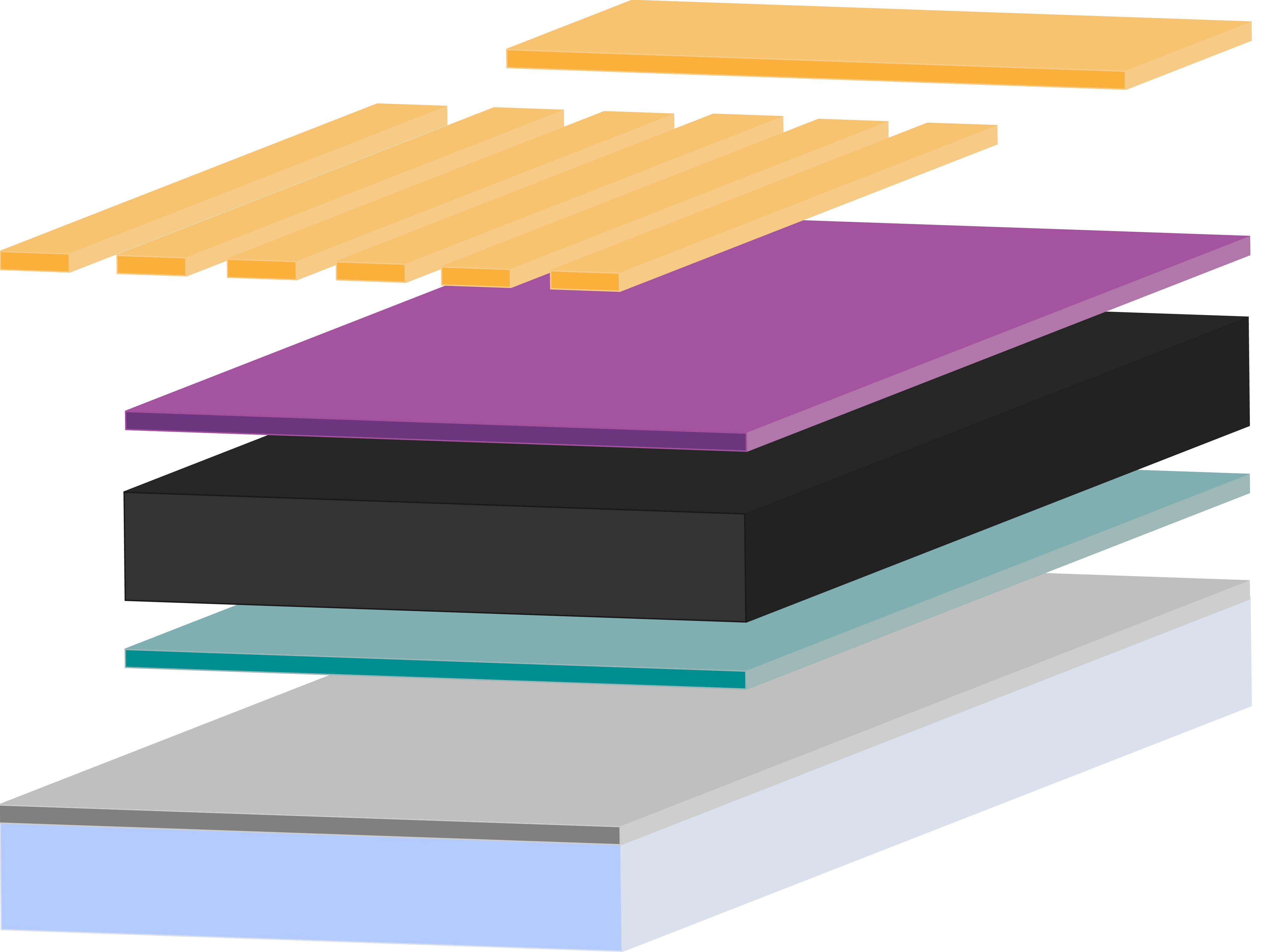
Perovskite solar cells (PSCs) need several layers in order to absorb light, then separate and extract charge. In basic terms, a planar PSC needs an absorbing perovskite layer sandwiched in between a hole transport layer and an electron transport layer.
Over the past 10 years, PSCs have achieved record efficiencies of 27.3% single junction solar cells (as of 20261). These efficiencies continue to rise due to perovskite's inherently low defect densities, tuneable bandgaps (making them perfect for tandem solar cells in conjunction with silicon-PV) and impressive optical and electronic properties. Perovskite solar cells can be almost completely solution processed and are compatible with roll-to-roll processing methods.
Constructing the highest performing PSCs requires the right perovskite materials selection, including choosing the right perovskite absorber layer matched with the best hole transport layer and electron transport layer. High efficiency devices also require carefully controlled processing of all layers.
Choosing Layers In A Perovskite Solar Cell
Choosing the best charge transport layers is extremely important when constructing an efficient perovskite solar cell. There are several factors to consider when making this decision, including:
- Processing limitations on substrates
- Band level alignments
- Device structure
- Wettability
- Chemical resistance of previous layers.
Good charge transport layers extract charge efficiently, while decreasing recombination losses at the transport layer/perovskite interface that may lower VOC2.
Structurally, depending on whether the device has an inverted or regular architecture, the “bottom” transport layer must be smooth, uniform and have good wettability to ensure that a smooth perovskite layer can be deposited on top of it.
Furthermore, the “illuminated” layers — through which light will need to pass to get to the perovskite absorber — must have good transparency to allow light through to the perovskite absorbing layer.
Example Perovskite Layers
Included here are recipes for making several different perovskite films and metrics of the solar cell devices made using these materials. All devices described here have the device stack:
ITO-Coated Glass /SnO2/perovskite material/Spiro-OMeTAD/Au
and these respective transport layers are deposited as described previously. All perovskite layers and hole transport layers were deposited in a glove box environment which maintained a level of <0.5% relative humidity and <0.5% O2.
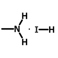
CsFAMAPb(IxBr1-x)3
We here examine a high-performing triple cation perovskite (CsFAMAPb(IxBr1-x)3) of 1.2M with a 4:1 DMF/DMSO solvent blend. Mixed halide (iodide, I, and bromide, Br) and mixed cation (methylammonium, MA, formamidinium, FA and cesium, Cs) PSCs have consistently produced devices with relatively impressive stability and durability. TC devices are acheive reasonably high efficiencies 25–27 and are very robust. Typically, these perovskites are processed in an inert environment to achieve the best performances, but nevertheless these perovskites are extremely versatile. In 2020, Bishop et al. demonstrated a fully sprayed PSC device using this TC ink, with small area efficiencies of 19.4%28, and this ink has been shown to be compatible incredibly scalable techniques such as air-blading quenching29. However, there are some issues with triple cation perovskites. For instance, methylammonium is extremely volatile, thermally unstable and will degrade in the presence of oxygen or moisture. Therefore, their use in PSCs can significantly lower the lifetime of the device. Nevertheless, when properly encapsulated, these PSCs have been shown to have great performance over several months.
Here, we have made devices using the aforementioned precursor, 50 µl of which was statically spin coated onto the SnO2-coated substrate with an Ossila Spin Coater using the following spin-anneal cycle:
| Step | Spin Speed | Duration | Comments |
|---|---|---|---|
| Ramp | 200 rpm/s | Until 2000 rpm is reached | |
| Spin 1 | 2000 rpm | 10 s | |
| Spin 2 | 4000 rpm | 30 s | Quench with 100 µl of antisolvent 20 s in |
| Anneal | 30 mins | Anneal at 100 °C |
During perovskite deposition, the Ossila Glove Box was continually circulating N2 compressed gas to avoid solvent build-up within the main chamber. Subsequently Spiro-OMeTAD and Au layers were deposited and devices were tested 2 days after perovskite and HTL deposition. When processing, all devices below <10% PCE or <0.5 VOC were removed. These results are summarized below. As can be seen in Figure 2, the average PCE over 6 devices of 6 pixels was 16.4±1.8 %. The highest PCE achieved by a single pixel was 19.0%, stabilizing at 17.6% over 1 minute.


Device metrics for 6 triple cation devices (left) and JV-sweep with fixed-power-point tracking for the best device
Tip: antisolvent quenching
One way to control crystallization during perovskite deposition is to use an anti-solvent quench method.
This involves depositing antisolvent material such as ethyl acetate, chlorobenzene or anisole, onto perovskite material while it is still spinning. This pushes volatile solvent such as DMF out of the lattice very quickly, whilst leaving other solvents which bond more strongly with the perovskite, such as DMSO, creating an intermediate phase. This residual solvent can be removed after via heat treatment, and this whole process has the effect of slowing down nucleation rate enabling a more uniform film to grow.
This process creates a very high-quality film, but it is not as easily scalable as vacuum-assisted processing and air-blading. Having said this, it is a useful technique for creating uniform films in the lab. The timing of the drop, choice of antisolvent and the amount of antisolvent used should be optimized for each perovskite stack. However, it is universally important that this “drop” should be slow, smooth, and continuous with no accidental drips.
MAPbI3
Methylammonium lead iodide (MAPbI3) is one of the earliest formulations of perovskite used in PSCs. Here, 1.1M methylammonium iodide (MAI) was dissolved with 1.1M of PbI2 in DMF. This is typically a high performing perovskite and can be processed at relatively low temperatures30. Their primary use of methylammonium as an A-cation can lead to some intrinsic instabilities, so although they may have impressive performance initially, this may deteriorate over a matter of days, if not properly encapsulated.
Again, we fabricated some devices using this perovskite precursor, 50 µl of which is statically spin coated onto SnO2-coated substrates using the following spin-anneal cycle:
| Step | Spin Speed | Duration | Comments |
|---|---|---|---|
| Spin 1 | 2000 rpm | 10 s | |
| Spin 2 | 5000 rpm | 30 s | Quench with 300 µl of antisolvent 20 s in |
| Anneal | 20 min | 100 °C |
These layers were deposited in our lab glove box. However, no circulation of N2 was needed to get optimum device performance. After spin coating, Spiro-OMeTAD and Au layers were deposited, and devices were tested one day after perovskite and HTL deposition. When processing, all devices below <10% PCE or <0.5 VOC were removed. The results are summarized below.
As can be seen in Figure 3, the average PCE over 3 devices of 6-pixels was 17.6±1.1 % with the champion PCE for a single pixel of 19.3%, stabilizing at 18.4% over 1 minute.


Device metrics of PSCs made from MAPbI3 precursor (left) and JV-sweep and stabilized-power-point tracking of the best device (right)
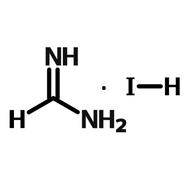
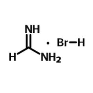
CsFAPbI3
Due to the various instabilities of methylammonium-based perovskites, formamidinium base perovskites (using halide salts such as formamidinium iodide or formamidinium bromide) are an appealing alternative. FAPbI3 has a smaller band gap than MAPbI3, which means it can absorb a larger proportion of the sun’s spectrum. This should lead to higher photocurrents and in turn better device efficiencies31.
However, FAPbI3 is phase-unstable and require high temperatures to convert fully to the black (α-) phase needed for perovskite solar cells, falling into a less absorbing, non-perovskite (β-) phase.
There has recently been a surge of formamidinium-based perovskites which show impressive device stability without the use of methylammonium cations to stabilize the α-perovskite phase. Currently (as of Nov 2021) the certified highest performance perovskite device is a doped FAPbI3-based perovskite achieving 25.5% PCE8 and there have been several other extremely successful examples using FAPbI3-based perovskites7,32,33 including a slot die coated device with an active area of 20.77 cm2 attaining PCEs of 16.6%32.
Here, we have fabricated some devices using this perovskite precursor, 50 µl of which is statically spin coated onto SnO2-coated substrates using the following spin-anneal cycle:
| Step | Spin Speed | Duration | Comments |
|---|---|---|---|
| Spin | 5000 rpm | 50 s | |
| Anneal 1 | 5 min | 70 °C | |
| Anneal 2 | 10 min | 150 °C outside the glove box |
During perovskite deposition, our laboratory glove box was continually circulating N2 to avoid solvent build up within the glove box chamber. Subsequently Spiro-OMeTAD and Au layers were deposited, and devices were tested 1 day after perovskite and HTL deposition. In processing, we removed all devices <10% PCE or <0.5 V VOC . Figure whatever shows the device metrics for all devices, along JV sweeps and fixed power tracking for the champion device.
The average device performance amongst seven devices was 14.0±2.0 % and the highest device sweep is 17.0% stabilizing at 16.0% after 1 minute.


Device metrics of PSCs made from CsFAPbI3 precursor (left) and JV-sweep and stabilized-power-point tracking of the best device (right)
I301
Here, we have fabricated some devices using our I301 triple cation perovskite ink. This uses dimethyl sulfoxide as the primary solvent making it a more stable perovskite solution34, but otherwise has the same stoichiometry as the previously mention triple cation ink (CsFAMAPb(IxBr1-x)3). 50 µl of which is statically spin coated onto SnO2 coated substrates using the following spin-anneal cycle:
| Step | Spin Speed | Duration | Comments |
|---|---|---|---|
| Spin 1 | 1000 rpm | 10 s | |
| Spin 2 | 3000 | 28 s | Quench with 100 µl of antisolvent after 18 s |
| Anneal | 10 min | 150 °C |
Here, all devices <10% PCE and <0.4 V Voc have been removed. We have used two different antisolvents during quenching to determine if this will significantly affect device performance. As can be seen here in Figure 6, it does not. The average device performance of I301 devices made using ethyl acetate as an antisolvent is 17.1±0.7% with a best performance of 18.5%, while those made with anisole as the antisolvent have an average PCE of 17.3±1.3% with a champion device of 19.4%. This demonstrates that high performance perovskite solar cells can be produced with a range of antisolvents.


Device metrics of PSCs made from I301 precursor (left) and JV-sweep of the best device (right)
Perovskite Materials Mentioned
Comparing Perovskite Devices
Here is a table comparing these PSCs. Here we have outlined how to fabricate good perovskite layers within a glove box environment and demonstrated that good PSCs can be formed with these layers.
| Perovskite | Average PCE (%) | Best PCE (%) |
|---|---|---|
| Cs0.05FA0.81MA0.14Pb(IxBr1-x) | 16.4±1.8 | 19.0 |
| MAPbI3 | 17.6±1.1 | 19.3 |
| CsFAPbI3 | 14.0±2.0 | 17.0 |
| I301 | 17.3±1.3 | 19.4 |
Electron Transport Layers
TiO2
Devices using a mesoporous TiO2 layer were popular in the early iterations of PSCs devices due to their use in dye-sensitized solar cells. TiO2 has reasonably good charge extraction properties and is also very chemically resistant2 so will not be affected by subsequent solvent processing.
Both compact and mesoporous TiO2 layers are still used in high efficiency PSCs. They often used together where a compact TiO2 layer ensures a full hole-blocking, electron-collecting layer while a mesoporous layer allows high levels of electron extraction.
However, these layers can require high temperature sintering (>400 °C) and are very time consuming to produce. Additionally, TiO2 has been shown to be vulnerable to UV light causing degradation of the perovskite layer3, which can sabotage device performance.
TiO2 can be doped with Ag or ruthenium to improve its performance as an ETL (by improving conduction, higher carrier mobility etc). For example, it has been shown that doping TiO2 with Ag alters the band gap hereby improving carrier transport properties4. Graphene-doped TiO2 led to a record PCE (in 2018) of 20.45% where it is determined that graphene provides a channel through the mesoporous TiO2 which can assist with electron extraction5. TiO2 has also been doped with rarer earth metals such as europium and samarium, and various other materials to improve band alignment and improve device stability2.
SnO2
SnO2 has a wider bandgap than TiO26 and its band alignment makes it perfect for charge extraction with methylammonium-based perovskites. Tin oxide also has high electron mobility in thin films and high chemical resistance, and can be processed using a range of low-temperature methods, such as chemical bath deposition7, spin coating, spray coating or slot die coating from nanoparticle suspensions6.
As of 2021, an SnO2 ETL has been used to achieve the certified world record highest efficiency PSC of 25.5%8. Here, in combination with a chlorine-heavy perovskite precursor, a chlorine-doped SnO2 interlayer is created between the SnO2 ETL and perovskite layer, increasing electron extraction. However, SnO2 layers do often require annealing at 150 °C, which could be a problem when working with some polymer substrates.
As this is a relatively low-stress ETL to fabricate, and can be made with an off-the-shelf nanoparticle solution, we have outlined a process for creating a compact SnO2 ETL below.
- Substrates should be placed in the UV-Ozone for at least 20 minutes before SnO2 deposition to ensure good wettability
- 15 wt% SnO2 nanoparticles are diluted in deionized water 4:1 and filtered immediately before use
- 50 μl of suspension is spin-coated statically at 3000 rpm for 30 s
- The layer is annealed at 150 °C for 30 minutes
ZnO
Zinc oxide is a low cost, low temperature alternative to TiO2 which makes it more appealing for commercialization. It is also more conductive than TiO2 and has a similar band gap.2 Although its ideal anneal temperature is 400 °C, it can be deposited by a sol-gel technique, which lowers this considerably. However, ZnO is chemically unstable at high temperatures, especially in conjunction with perovskite material2.
ZnO layers can also be doped with different materials to counter defects at the ZnO/perovskite interface. For example, Azmi et al. achieved an impressive PCE of 19.9% when using potassium doped ZnO in stark contrast to their 16.10% devices using only ZnO as an ETL.9
PCBM
Phenyl-C61-butyric acid methyl ester (PCBM) is a material that will form a stable ETL and can be easily solution processed on top of a perovskite layer, making it ideal for inverted perovskite solar cells.
For this reason, it was very popular in the early days of PSCs. However, several issues with this material ultimately limit device performance. Rough morphology of the perovskite layer can lead to an uneven layer of PCBM, creating a hot spot for non-radiative recombination. To reduce this effect, PCBM can be used in conjunction with other transport layers such as C60 and LiF10.
Alternatively, PCBM can be doped to improve film morphology and to better match energy layers within the device. In 2019, Yang et al. doped pure PCBM with an n-type polymer F9TBT11, which considerably improve coverage of the combined ETL, yielding an inverted MAPbI3 devices of 20.6%.
C60
C60 is a fullerene material that can make a compact transport layer, with higher electron mobility than other ETLs used in inverted devices such as PCBM.11 They can also be used in either regular or inverted devices. Due to their improved film morphology compared to PCBM, C60-based devices exhibit low levels of hysteresis, which is an important property for inverted perovskite devices. Often, they are used in conjunction with a BCP hole-blocking layer, which allows for better charge selection at the electron transport interface.
Hole Transport Layers
Spiro-OMeTAD
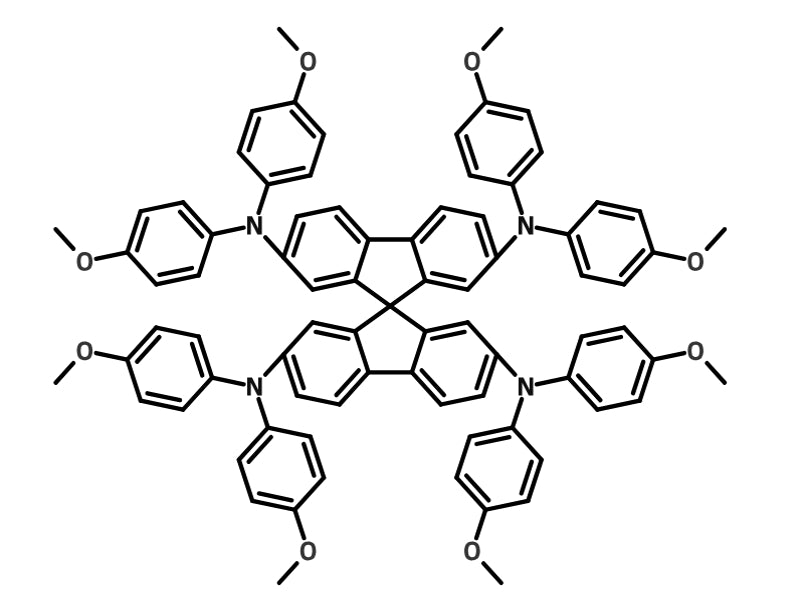
Spiro-OMeTAD is one of the most used hole-transport layers for PSCs. It regularly produces high efficiency PSCs — and is used in the current world champion device8.
Spiro-OMeTAD can be purely solution processed and has no annealing step, meaning it can be processed easily at low temperatures. In fact, a Spiro-OMeTAD HTL has been shown to be compatible with large scale perovskite production, with Di Giacomo et al. creating >15 cm2 devices with over 10% PCE12 and Kim et al. showing that devices using Spiro-OMeTAD created with completely roll-to-roll processes have a champion PCE of 13.8%13.
However, Spiro-OMeTAD requires the addition of several dopants to achieve maximum conductivity, hole mobility and to ensure these dopants dissolve in chlorobenzene. Additionally, there is mounting evidence suggesting Spiro-OMeTAD may provide long term stability issues with PSC devices14. This deterioration has been linked with the aforementioned dopants, so much research is looking at replacing these dopants with Zn-TFSI, Mg-TFSI2 and Ca-TFSI2 and so far, promising improvements have been seen in device stability.
As Spiro-OMeTAD is the most used HTL, we have outlined our favorite recipe for creating the perfect "Spiro" layer in a regular perovskite solar cell architecture.
- 85 mg/ml of Sublimed Spiro-OMeTAD (<99.5% purity) is dissolved in chlorobenzene and left to dissolve fully for 2 hours.
- Dopants are added to this in stock solution in the following order:
- LiTFSI: 20 μl/ml from a 500 mg/ml stock (dissolved in ACN) added and vigorously dissolved for 1 minute
- tBP: 34 μl/ml from stock solvent and dissolved for 1 minute.
- Fk209 Co(III) TFSI Salt : 11 μl/ml from a 300 mg/ml stock (dissolved in ACN) added and dissolved for 1 minute.
- This layer should be deposited in an inert environment like a laboratory glove box and the solution should be filtered promptly before deposition with a 0.2 µm filter.
- 25 μl of this solution should be dynamically spin coated onto the perovskite layer at 4000 rpm for 30 s. These should then be left in a dark, dry atmosphere in air overnight before further processing to allow the Spiro-OMeTAD to oxidize fully.
PTAA
Poly[bis(4-phenyl)(2,4,6-trimethylphenyl)amine (PTAA) is another hole transport layer for PSCs. It has many of the same qualities as Spiro, in that it is a small organic molecule with which impressive perovskite solar cells have been achieved, but usually dopants are needed to achieve these high performances — the same dopants that are problematic in Spiro-OMeTAD devices i.e. LiTFSI. Therefore, more stable dopants (such as Lewis Acid Dopants) have been used to create PTAA-perovskite devices with PCE of >19% that show good device stability15.
It has also been demonstrated that dopant-free PTAA can been used in inverted devices along with PCBM as an ETL, and these devices also show good performance16.
PEDOT:PSS
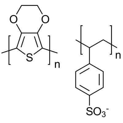
PEDOT:PSS (Poly(3,4-ethylenedioxythiophene) polystyrene sulfonate) has often been used in inverted perovskite solar cell devices and was used in the first solid PSC device, achieving efficiencies of 3.8%17.
PEDOT:PSS has good wettability, good solubility in greener solvents and is quite transparent in the visible region.18 However, it suffers from low conductivity - as the PSS part of the molecule as an isolating agent in the layer- and the material suffers from mismatched energy levels with most perovskite material.
Additionally PEDOT:PSS will absorb ambient moisture, which can wreak havoc when in a perovskite stack. Doping PEDOT:PSS with various things can improve the materials charge carrier dynamics, work function and the overall film morphology, all of which lead to a better PSC. However, the challenge remains to improve all these properties at the same time.
As of 2019, the highest perovskite solar cell efficiency achieved using this HTL involves doping the PEDOT:PSS with CsI19. This lowers the work function of the HTL, reducing the energy barrier between PEDOT:PSS and the perovskite, hereby increasing hole extraction. Xhang et al. found that PEDOT:PSS doped with NiPcS4 results in a slightly higher work function than PEDOT:PSS alone20. However, this doping also significantly increases the lowest unoccupied molecular orbit (LUMO) which enables necessary electron blocking through the layer.
In turn, this leads to a higher JSC, and better and more stable devices.
Self-Assembled Monolayers
Self-assembled monolayers (SAMs) are the general name for 2D nanomaterials that are only one molecule thick. SAM molecules, such as MeO-2PACz will self-assemble into organized layers21. They consist of three parts – terminal molecule that interacts with the perovskite, an anchor molecule that attaches the SAM to the adjacent layer and a spacer molecule in between that helps enable the organization of the film.

Within perovskite solar cells, the work function of the hole and electron transport layers must be carefully optimized to enable extraction of one charge whilst blocking the movement of another. For this purpose, SAMS can be very useful as interlayers, as their electrical properties can be easily tailored21. They can also help improve the crystallization of the perovskite layer for a more efficient device.
Additionally, SAMs can be solution processed so can be immediately incorporated into most PSC devices. A wide range of SAMS have been used for different purposes within perovskite devices, we will outline a few here that assist with charge transport. For a more thorough review of how SAMs can improve other perovskite features, such as morphology, read on here21.
A SAM layer has been used to reduce the gathering of positive ions at perovskite/SnO2 interfaces that would encourage non-radiative recombination22. SAMS have also been used as the main hole transport material in inverted PSC devices which have been shown to outperform PEDOT:PSS HTLs23 and can certainly compete with PTAA HTLs in terms of stability24.
Energy Level Diagrams in Perovskite Solar Cells

Band level alignment to extremely important in perovskite solar cells. Figure 1 shows the band gap for several hole and electron transport layers, as well as several perovskites. When the perovskite absorber captures a photon, this results in both an electron in the conduction band (CB) and a "hole" in the valence band (VB). It is important to extract these charges from their respective layers as quickly as possible to avoid recombination.
The electron that is occupying a space in the perovskite's conduction band must be able transfer easily into the conduction band of the electron transport layer. If the conduction band of a material is at a higher energy level than the perovskite's conduction band, however, there will be an energy barrier preventing this movement of electrons.
It is therefore beneficial that the conduction band of the electron transport layer is lower than that of the perovskite. This allows the electron to passively diffuse away from the perovskite.
In the hole transport layer, the energy level of the valance band should be close to or slightly higher than the perovskite's valance band so that electrons can quickly diffuse into the unoccupied "holes" in the perovskite before recombination occurs.
Tip: pixel area
Substrates can be patterned in several different ways. Pre-patterned ITO substrates can be used to make 8-pixel devices, while unpatterned devices can be etched to be compatible with 1-pixel or 6-pixel architectures. To help choose your pixel area/device structure, think of what you stage you are at with your investigation.
8-pixel or 6-pixel substrates have small pixel area but allow you to extract data from the good areas of a device. This also gives you higher statistics for less devices. It is useful for screening a lot of factors in one experiment.
1-pixel devices have a larger device area and will better represent the PSC as it should be used. The field in general is moving towards the goal of at least 1cm2 device areas to compete with other PV technologies. However, one small pinhole/defect and the whole device will short.
It is therefore common to begin the experimental process using smaller device areas, then do larger area device runs for champion data, for publication or when focusing on the scalability of a material or technique.
Perovskite Materials

Learn More
 Perovskite Solar Cells vs Silicon Solar Cells
Silicon is the most commonly used material in photovoltaic (PV) technology. In recent times perovskite materials have generated much excitement in the field of solar cell research. Here we discuss the pros and cons of each in addition to their use in conjunction with one another.
Read more... What are Self-Assembled Monolayers (SAMs)?
A self-assembled monolayer (SAM) is a well-organized, one molecule thick layer that forms on a solid surface. SAM molecules, like MeO-2PACz, adsorb on a substrate via chemical or physical bonds.
Read more...References
- Best Research-Cell Efficiencies, National Renewable Energy Laboratory, (2020); DOI: 10.1016/j.jet.2007.03.008.
- Metal Oxide Electron Transport Materials For Perovskite Solar Cells: A Review, K. Valadi et al., Environ. Chem. Lett., 19 (3), 2185–2207 (2021); DOI: 10.1007/s10311-020-01171-x.
- Organometal Halide Perovskite Solar Cells: Degradation And Stability, T. A. Berhe et al., Energy Environ. Sci., 9 (2), 323–356 (2016); DOI: 10.1039/C5EE02733K.