FREE shipping to on qualifying orders when you spend or more, processed by Ossila BV. All prices ex. VAT. Qualifying orders ship free worldwide! Fast, secure, and backed by the Ossila guarantee. It looks like you are visiting from , click to shop in or change country. Orders to the EU are processed by our EU subsidiary.

It looks like you are using an unsupported browser. You can still place orders by emailing us on info@ossila.com, but you may experience issues browsing our website. Please consider upgrading to a modern browser for better security and an improved browsing experience.

Perovskite Precursor Ink for Air Processing

Perovskite Inks, Perovskite Materials


Product Code I101
Price £200 ex. VAT

Quality assured

Expert support

Volume discounts

Worldwide shipping

Fast and secure


Perovskite precursor ink for the fabrication of solar cells to achieve high PCE values

High quality ink with the ability to be processed in an ambient environment


I101 perovskite ink has been specially formulated in the Ossila laboratories to be deposited by spin coating. Our I101 perovskite ink is designed for air processing in low-humidity environments. Using a mixture of methyl ammonium iodide (MAI) and lead chloride (PbCl2) dissolved in dimethyl formamide, our I101 perovskite ink will convert to a methylammonium lead halide perovskite under heat. The final product is a methylammonium lead iodide perovskite with trace amounts of chlorine given by the formula CH3NH3PbI3-xClx. For information on the various applications of the mixed halide CH3NH3PbI3-xClx perovskite see our applications section.

The main use of CH3NH3PbI3-xClx is in the fabrication of solar cells, our I101 ink can be used in both standard and inverted architectures; and can achieve power conversion efficiency (PCE) values of over 13% (see our device performance section for more information). The ink specifications can be found below along with complete guides on the processing of perovskite inks for standard architecture and inverted architectures. Using our I101 recipe provided, 5ml of solution is capable of processing up to 160 substrates (1,280 devices using our 8-pixel substrate design).

Perovskite Ink
I101 is packaged as 10 individual vials containing 0.5 ml of solution capable of coating up to 160 substrates. I101 can also be bought in bulk (30 ml) with a 25% discount over our standard order sizes.

Specifications

Perovskite Type CH3NH3PbI3-xClx
Precursor Materials Methyl Ammonium Iodide (99.9%), Lead Chloride (99.999%)
Precursor Ratio 3:1
Solvent Dimethyl Formamide (99.8%)
Optical Bandgap 1.56 – 1.59 eV
Energy Levels Valence Band Minimum 5.4 eV, Conduction Band Minimum 3.9 eV
Emission Peak 770 – 780 nm (PL); 755 – 770 nm (EL)
Standard Architecture PCE 13.7% Peak; 13.0% ±0.25% Average
Inverted Architecture PCE 13.1% Peak; 11.9% ±0.50% Average
Processing Conditions Air processing; low humidity (20% to 35%)
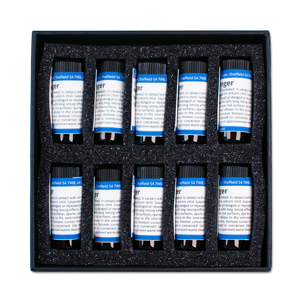
Packaging 10 x 0.5 ml sealed amber vials; 3 x 10 ml sealed amber vials

I101 Perovskite Applications

Perovskite Photovoltaics

The single biggest application of perovskite materials is for photovoltaic devices; perovskites fabricated from MAI:PbCl precursors have been used in several papers to achieve high power conversion efficiencies. The advantage of using MAI:PbCl as precursor materials is the ability to process in an ambient environment.

Perovskite LED and Lasing

Due to the high photoluminescence quantum yield of perovskites at room temperature, the application of these materials in light-emitting diodes (LEDs) is of great interest. Devices made using MAI:PbCl precursors show strong emission in the near-infrared region at 755 nm. Additionally, recent work has shown lasing within this material.

Scale-Up Processing

Due to the ability to process perovskites based upon MAI:PbCl precursors in air, the material opens up the possibility of applications in large-scale deposition techniques. Several different scalable techniques, such as slot die coating and spray coating have been used to deposit this material.

I101 Perovskite Processing Guides

Standard Architecture:

FTO/TiO2(Compact)/TiO2(Mesoporous)/I101/Spiro-OMeTAD/Au

Below is a condensed summary of our fabrication routine for standard architecture devices using our I101 ink.

  1. FTO etching:
  • A complete guide to FTO etching can be found on our FTO product page along with an instructional video
  1. Substrate cleaning:
  • Sonicate FTO for 5 minutes in hot (70 °C) DI water with the addition of 1% Hellmanex
  • Dump-rinse twice in boiling DI water
  • Sonicate FTO for 5 minutes in Isopropyl alcohol
  • Dump-rinse twice in boiling DI water
  • Dry FTO using filtered compressed gas
  • Place the FTO into the UV Ozone Cleaner and leave for 10 minutes

UV Ozone Cleaner

Ossila UV Ozone Cleaner
  • Ultraclean Surfaces within Minutes
  • Built-In Software

Buy Online £2,500

  1. Compact TiO2 deposition:
  • Prepare a solution of titanium diisopropoxide bis(acetylacetonate) at a volumetric percentage of 8% in isopropyl alcohol (approximately 20 ml will be needed)
  • Mask off the substrates such that only the active area of the devices are exposed
  • Place the substrates onto a hotplate set to 450 °C
  • Using a nitrogen/compressed air gun set it to a pressure of 16 – 18 psi and spray the solution onto the substrates. Leave the solution for 30 seconds to dry, and sinter and repeat the spray process again. Repeat this until you get approximately 40 nm of film, this should take around 10 sprays
  • Cover the substrates loosely with foil and leave to sinter for 30 minutes
  • After sintering remove the substrates from the hotplate, care should be taken as rapid cooling can shatter the substrate
  1. Mesoporous TiO2 deposition:
  • Using a mesoporous paste with a particle size of 18 nm and pore size of 30nm, prepare a mesoporous film of approximately 200 nm thick
  • Place the substrates back on the hotplate, loosely cover with foil and sinter the substrates at 450 °C for 1 hour
  • After sintering remove the substrates from the hotplate, care should be taken as rapid cooling can shatter the substrate
  1. Perovskite deposition (in air):
  • Heat I101 ink for at least 2 hours at 70 °C to allow for complete redissolution of solutes
  • Allow I101 ink to cool to room temperature before deposition
  • Set the hotplate temperature to 90 °C
  • Static spin coating: place substrate into spin coater, dispense 30-50 μl and start spinning at 2000 rpm for 30 s
  • Place substrate onto the hotplate and anneal for 120 minutes
  • After annealing, transfer the substrates into a glove box environment.

Spin Coater

  • Vacuum-Free Design
  • Compact Size
  • No Substrate Warping

Available From £2,100

  1. Spiro-OMeTAD deposition (in air):
  • Prepare the following solutions; Spiro-OMeTAD at a concentration of 97 mg/ml in chlorobenzene, Li-TFSI at a concentration of 175 mg/ml in acetonitrile, and TBP at a volumetric percentage of 46.6% in acetonitrile
  • Combine 1000 μl Spiro-OMeTAD, 30.2 μl Li-TFSI, and 9.7 μl TBP solutions
  • Dispense 50 µl of the combined solution onto the perovskite, allowing it to spread across the substrate
  • Spin at 2000 rpm for 30 seconds
  • Use a high-precision mirco cleaning swab soaked in chlorobenzene to wipe the cathode strip clean
  1. Spiro-OMeTAD oxidation and anode deposition:
  • Place the substrates inside a desiccator in air and leave the substrates for 12 hours in the dark to allow for oxidation of the spiro-OMeTAD film (The amount of time required for complete oxidation of the spiro-OMeTAD may vary depending upon thickness and environmental conditions. Additional oxidation steps may be needed after deposition of anode)
  • Using thermal evaporation, deposit an 80 nm layer of gold through a shadow mask to define an active area for your device
  • Devices do not need to be encapsulated for measuring performance
  • If encapsulation is desired, the spiro-OMeTAD should be allowed to fully oxidise again before substrates are transferred into the glove box and encapsulated

Inverted Architecture:

ITO/PEDOT:PSS/I101/PC70BM/Ca/Al

For a complete step-by-step guide please see our full perovskite solar cells fabrication guide or our instructional video guide below.

Below is a condensed summary of our routine, which is also available to download as a PDF to enable you to print and laminate for use in the clean room.

  1. Substrate cleaning:
  • See substrate cleaning section of standard architecture device guide
  1. PEDOT:PSS deposition:
  • Filter PEDOT:PSS using a 0.45 µm PES filter
  • Dispense 35 µl of the filtered PEDOT:PSS solution onto ITO spinning at 6000 rpm for 30 s
  • Place substrate onto a hotplate at 120 °C
  • After all ITO substrates are coated, reduce the hotplate temperature to 90 °C
  1. Perovskite deposition (in air):
  • Heat I101 ink for at least 2 hours at 70 °C to allow for complete re-dissolution of solutes
  • Transfer heated substrate onto spin coater, start spinning at 4000 rpm and dispense 30 μl of I101 ink and leave to spin for 30 s
  • Place substrate back onto the hotplate at 90 °C for 120 minutes
  • After annealing transfer the substrates into a glove box environment.
  1. PC70BM deposition (in nitrogen glove box):
  • Prepare a solution of PC70BM at 50 mg/ml in chlorobenzene and stir for 3 to 5 hours
  • Transfer perovskite-coated substrates into the glove box
  • Dispense 20 µl of PC70BM solution onto the spinning substrate at 1000 rpm and spin for 30 s
  • Use a micro-precision cleaning swab soaked in chlorobenzene to wipe the cathode strip clean
  1. Cathode deposition:
  • Using thermal evaporation, sequentially deposit 5 nm of calcium and 100 nm of aluminium through a shadow mask to define an active area for your device
  • Encapsulate devices using a glass coverslip and encapsulation epoxy
  • Expose to UV radiation (350 nm) for ~5 minutes (times vary depending upon source intensity) to set the epoxy

I101 Device Performance

Below is information on photovoltaic devices fabricated using our standard architecture and inverted architecture recipes for I101 inks. All scans were taken after 10 minutes under illumination of an AM1.5 source, using a voltage sweep from -1.2 V to 1.2 V then from 1.2 V to -1.2 V at a rate of 0.2 V.s-1; no bias soaking was performed on devices.

Architecture Standard Inverted
Sweep Direction Forward Reverse Forward Reverse
Power Conversion Efficiency (%) 13.5 13.7 12.4 13.1
Short Circuit Current (mA.cm-2) -20.8 -20.8 -18.8 -18.8
Open Circuit Voltage (V) 0.88 0.90 0.96 0.96
Fill Factor (%) 73 73 69 72
I101 standard and inverted architecture perovskite solar celll iv curves
JV curve under AM1.5 irradiation for a standard (left, courtesy of Michael Stringer-Wong, University of Sheffield) and inverted (right, courtesy of Alex Barrows, University of Sheffield) device based on Ossila's I101 ink. Device characteristics were recorded on a reverse sweep.

References

Perovskite Photovoltaics

  • Efficient hybrid solar cells based on meso-superstructured organometal halide perovskites. J. Snaith et. al. Science. 338 (2012) 643-647 DOI: 10.1126/science.1228604
  • Additive enhanced crystallization of solution-processed perovskite for highly efficient planar- heterojunction solar cells. K-Y. Jen et. al. Adv. Mater. 26 (2014) 3748-3754 DOI: 10.1002/adma.201400231
  • Morphological control for high performance, solution-processed planar heterojunction perovskite solar cells. J. Snaith et. al. 24 (2014) 151-157 DOI: 10.1002/adfm.201302090

Perovskite LED and Lasing

  • Bright light-emitting diodes based on organometal halide perovskite. R. H. Friend et. al. Nature Nanotechnology, 9 (2014) 687-692 doi:10.1038/nnano.2014.149
  • Interfacial control towards efficient and low-voltage perovskite light-emitting diodes. Hang et. al. Adv. Mater. 27 (2015) 2311-2316 DOI: 10.1002/adma.201405217
  • High photoluminescence efficiency and optically pumped lasing in solution-processed mixed halide perovskite semiconductors. H. Friend et. al. J. Phys. Chem. Lett. 5 (2014)1421-1426 DOI: 10.1021/jz5005285

Scale-Up Processing

  • Upscaling of perovskite solar cells: Fully ambient roll processing of flexible perovskite solar cells with printed back electrodes. C. Krebs et. al. Adv. Energy Mater. 5 (2015) 1500569 DOI: 10.1002/aenm.201500569
  • Highly efficient, felixble, indium-free perovskite solar cells employing metallic substrates, M. Watson et. al. J. Mater. Chem. A, 3 (2015) 9141-9145 DOI: 10.1039/C5TA01755F
  • Efficient planar heterojunction mixed-halide perovskite solar cells deposited via spray-deposition. G. Lidzey et. al. Energy Environ. Sci. 7 (2014) 2944-2950 DOI: 10.1039/C4EE01546K
Return to the top