Perovskite Precursor Ink for Nitrogen Processing
Specially formulated, high quality perovskite precursor ink
For the fabrication of photovoltaic devices under a nitrogen atmosphere
Overview | Specifications | Example Device Data | Fabrication Method | References
A formulation of methylammonium iodide (MAI), PbCl2 and PbI2 at a molar ratio of 1:1:4 (PbCl2:PbI2:MAI) in a DMF solvent. On processing, I201 ink can be used to create a CH3NH3PbI3-xClx perovskite film. The process recipe for I201 is optimized for glove box processing under a nitrogen atmosphere.
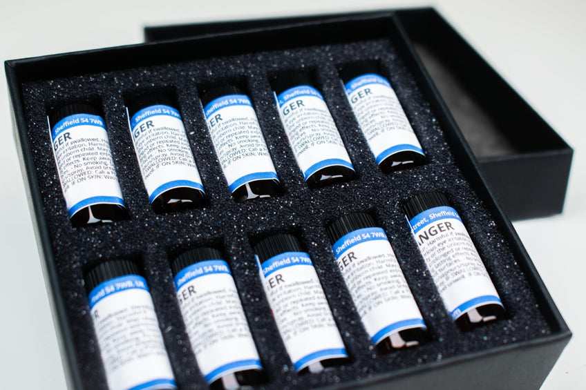
I201 perovskite ink is divided into 10 lots of 0.5 ml. We have found this quantity to be sufficient for 10 individual experiments (approximately 160 device substrates).
Datasheet
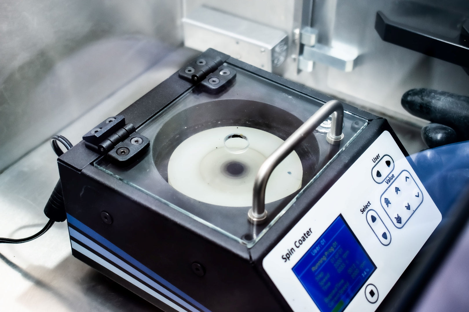
We have specially formulated I201 Perovskite Ink in our laboratories to make it suitable for deposition using a spin coater. It is based on similar ink formulations used in references [1]. This ink is designed to be used with a bottom ITO/PEDOT:PSS AI 4083 anode and a top PC70BM/Ca/Al cathode, with PV devices fabricated with an average / peak power conversion efficiency (PCE) of (11.2% ± 0.4)% / 11.8%. This performance level is in accord with other literature reports using similar ink formulations where PCEs of approximately 11.5% have been demonstrated [1]. A full process recipe comes with the ink, which is ready to use after heating for a short time.

Specifications
Perovskite precursor ink formulation: Ink I201 is based on a mixture of methylammonium iodide (MAI), lead chloride (PbCl2) and lead iodide (PbI2) at a molar ratio (PbCl2:PbI2:MAI) of 1:1:4 dissolved in anhydrous DMF (dimethylformamide).
| Compound | Purity | Molar Ratio |
|---|---|---|
| MAI | > 99% (as measured by Elemental Analysis) | 4 |
| PbCl2 | 99.999% | 1 |
| PbI2 | 99.999% | 1 |
| DMF | 99.8% | N/A |

Perovskite Photovoltaic Device Performance
Below are device characteristics for our best pixel fabricated using the I201 fabrication recipe described above.
JV curves demonstrate the hysteresis observed from the device and include device metrics for both forward and reverse sweeps. The pixel presented (from a reverse sweep) had a power conversion efficiency of 11.8%, a Voc of 0.91 V, a FF of 79% and a Jsc of -16.5 mA/cm2.


Suggested Fabrication Method
 I201 Nitrogen-Processed Perovskite Solar Cell Fabrication
The summary below outlines the key steps required when processing I201 Perovskite Ink. You can also download this summary as a PDF in order to print and laminate it for use in a clean room.
Read more...References
- Reproducible One-Step Fabrication of Compact MAPbI3-xClx Thin Films Derived from Mixed-Lead-Halide Precursors, D. Wang et al., Chem. Mater., 26, 7145-7150 (2014) DOI: 10.1021/cm5037869
