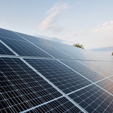
Organic Solar Cells: An Introduction to Organic Photovoltaics

Organic solar cells, also known as organic photovoltaics (OPVs), have become widely recognized for their many promising qualities, such as:
- Ease of solution processability
- Tuneable electronic properties
- Possibilities for low temperature manufacturing
- Cheap and light materials.
Whilst several other photovoltaic technologies have higher efficiencies, OPVs remain advantageous due to their low material toxicity, cost, and environmental impact. They have exceeded certified efficiencies of 19.2% (Zhu et al. 2022) , putting them in fierce competition with both inorganic and hybrid organic-inorganic PV technology.
What is an Organic Solar Cell?
An organic solar cell (also known as OPV) is a type of solar cell where the absorbing layer is based on organic semiconductors (OSCs). Typically, these are either semiconducting polymers or small molecules. For organic materials to be used in organic electronics, they will need to be semiconducting which will require a high level of conjugation (alternating single and double bonds). Conjugation of the organic molecule results in the electrons associated with the double bonds becoming delocalised across the entire length of conjugation. These electrons have higher energies than other electrons in the molecule and are similar to valence electrons in inorganic semiconductor materials.
However, in organic materials, these electrons do not occupy a valence band but are part of what is called the ‘highest occupied molecular orbital’ (HOMO). Just like in inorganic semiconductors, there are unoccupied energy levels at higher energies. In organic materials, the first one is called the lowest unoccupied molecular orbital (LUMO). Between the highest occupied molecular orbital (HOMO) and lowest unoccupied molecular orbital (LUMO) of the OSC is an energy gap - often referred to as the band gap of the material. With increased conjugation, the band gap will become small enough for visible light to excite an electron from HOMO to LUMO.
How do Organic Solar Cells Work?
As with other solar cell technologies, the purpose of an organic solar cell is to generate electricity from sunlight. This is achieved when the energy of light is equal to or greater than the band gap, leading to absorption and excitation of an electron from the HOMO to the LUMO. The excited electron will leave behind a positively-charged space known as a ‘hole’. Due to the opposite charges of the hole and electron, they become attracted and form an electron-hole pair, also known as an ‘exciton’. To remove the charged particles from the solar cell, the electron-hole pair must be separated, and this process is known as ‘exciton dissociation’.
Typically in an inorganic semiconductor, the attraction between the electron and hole (known as the exciton binding energy, Eb) is small enough to be overcome by thermal energy at room temperature, approximately 26 meV (Yan, 2018). This is due to a high dielectric constant — meaning there is significant screening between the electron and hole, reducing the attraction between them. The ease in separating the electron and hole allows easy exciton dissociation.
In contrast, OSCs have low dielectric constants, giving large Eb values in the range of 0.3–0.5 eV (Brabec, 2010). In OSCs, exciton dissociation cannot be achieved by thermal energy alone. To overcome this, at least two different OSCs are needed within an OPV. The energy levels between the two different OSCs are offset, with the difference being greater than Eb, allowing exciton dissociation to occur at the interface between them.
Depending on how the exciton dissociates, the OSCs are classified as either a ‘donor’ or ‘acceptor’ (referring to whether the electron has been donated by a material or accepted by a material). In most OPVs, the donor will absorb the most light, and therefore the exciton will be generated on this material. At the interface with the acceptor, the exciton will dissociate. The electron will be donated to the acceptor material, which has a deeper HOMO and LUMO level, whilst the hole remains on the donor material.

The steps that govern organic solar cell function can be summarised as:
1. Absorption of incident, light leading to exciton generation
Light with enough energy will be absorbed by the OSC and excite electrons from the HOMO to the LUMO to form an exciton. If the energy of light being absorbed is greater than the band gap, the electron will move to a higher energy level than the LUMO and decay down. This process is known as ‘thermalization’ (or thermalisation) during which the energy is lost as heat. Thermalization is a key energy-loss mechanism in photovoltaics.
2. Diffusion of the exciton to a donor-acceptor interface
Once formed, the exciton diffuses through the OSC component to the donor-acceptor interface, where the offset between LUMO levels will drive exciton dissociation. This must occur within a certain amount of time. If not, the excited electron will return to the empty energy state (known as the hole), a process known as ‘recombination.’ The time taken is known as the ‘exciton lifetime,’ which is often represented as the distance that the exciton can diffuse in this time (which is around 10 nm).
3. Dissociation of the exciton across this interface
At the interface, the electron will move to the acceptor material and the hole will remain on the donor. These charge carriers will still be attracted, and so form a charge-transfer state. When the distance between the pair increases, the attraction decreases. Eventually, the binding energy between them is overcome by thermal energy, and a charge-separated state is formed. While the electron-hole pair are still attracted in the charge-transfer state, recombination can occur across the interface between the two materials.
4. Charge-carrier transport
The charge-carriers will then diffuse to the appropriate electrodes (i.e. the holes to the anode and electrons to the cathode) through the relevant interfacial layers.
5. Charge-carrier collection
At the electrodes, the charge carriers are collected and used to do work in the external circuit of the cell – producing a current.

Recombination
At several stages, the electron and hole can recombine — at which point the absorbed energy used for initial excitation is wasted.
Recombination can be categorised as either:
- Geminate — The initially-produced electron-hole pair recombine before exciton dissociation
- Non-geminate — Free electrons and holes can recombine, regardless of their source
Both of these processes can be radiative, where a photon is released, or non-radiative, where a photon is not released (Menke et al, 2018). Non-radiative processes include trap-assisted recombination, where structural defects result in the formation of energy states in the gap between the HOMO and LUMO.
The Development of Organic Solar Cells
The first two-component OPV was proposed by Tang (1986) but efficiencies remained very low for several years due to the reliance on bilayer cells. Excitons can only dissociate at the interface between donor and acceptor, and can generally only diffuse approximately 10 nm before decaying back to the ground state (Brabec et al, 2010). In contrast, a total active layer thickness of above 100 nm is usually required to absorb light efficiently — meaning bilayer cells are either too thin to properly absorb, or too thick for efficient exciton dissociation.
The solution to this was proposed in 1995, and is known as the bulk heterojunction (BHJ) cell (Halls et al, 1995; Yu et al, 1995). Here instead of a strict two-layer system, the donor and acceptor materials are intimately mixed at the nanoscale level — allowing interfaces at an appropriate diffusion distance to be dispersed across the active layer whilst maintaining the necessary thickness for absorption.

Since this time, there have been countless refinements in morphology control (Huang et al, 2014; Shaheen et al, 2001), development of new donors (Holliday et al, 2017; Ma et al, 2005; Leonard et al, 2022; Park et al, 2009), new acceptors (Cheng et al, 2018; Hou et al, 2018; Leonard et al, 2022) and technical expertise, leading to modern BHJ OPVs exceeding certified efficiencies of 19% (Zhu et al, 2022).
The majority of OPVs used in modern research are solution-processed BHJ cells, where the architecture can be classified as conventional or inverted, depending on the orientation of the electrodes (see figure). With the discovery of highly absorbent non-fullerene acceptors and complementary donor materials, there is some re-examination of bilayer OPV devices, especially for usage in situations with low light intensities such as for indoor photovoltaics (Park et al, 2021). However, BHJ solar cells remain the most reliable way to produce a high efficiency solar cell particularly under 1 Sun illumination. Therefore, we will discuss mainly BHJ structures in this guide.

In most cases, OPVs must use at least two OSC materials in order to create a successful OPV active layer. Although, some interesting examples of single component OPVs have been explored (Liang et al, 2023; Wu et al, 2017). However, some research has found that incorporating a third OSC material can improve device performance. By selectively interacting with either the donor or acceptor material, this ternary OSC can introduce some morphological control into film formation. Ternary OPV devices have shown PCEs > 19% with improved illumination stability compared to binary devices1.
Charge-carrier transport is facilitated through the device using hole-and electron-transporting interfacial layers on either side of the active layer. A typical hole-transporting layer (HTL) in a conventional stack could be PEDOT:PSS, often paired with an ITO anode, whilst a typical electron-transporting layer (ETL) could be PFN-Br or bathocuproine (BCP), often paired with a metal cathode (either silver, gold or aluminium). These layers facilitate the movement of one type of charge carrier by positioning energy levels favorably, while hindering the transport of the other carrier. These kinds of layers can therefore be utilized as electron or hole blocking layers, preventing charge movement in the wrong direction.

Non-Fullerene Acceptors in Organic Solar Cells
For many years, the majority of acceptors used were derived from fullerene and the most commonly used donor:acceptor OPV materials were P3HT:PCBM. However, the introduction of non-fullerene acceptors (NFAs), especially those based on small molecules, has revitalized the OPV field. NFA-OPVs have yielded higher efficiencies (Zhu et al, 2022) and stabilities (Cha et al, 2017) than fullerene-based acceptors, breathing new life into the field.
One of the main limitations of fullerene acceptors is that they cannot be modified without changing their conjugation, affecting their optoelectronic properties. This means that they are confined to exhibit poor light absorption in the visible region. NFAs can be easily modified to adapt their absorption properties, solubility and stability. Therefore, NFA-OPVs can be highly absorbing, allowing plenty of exciton generation in both the donor and acceptor components of the active layer.
Non-Fullerene Acceptor materials fall into three broad categories (Leonard et al, 2022):
- A-D-A fused ring acceptors (such as ITIC, IT-2F, ITIC-4Cl and other derivatives) –These molecules consist of a backbone and sidechains, both of which can be modified to change their molecular or optoelectronic properties. ITIC is probably the most used commonly NFA in OPVs over the past 5 years.
- Y-series (or A-DAD-A) small molecules (such as Y6/BTP-4F or Y7/BTP-Cl) – small molecules with an A-DAD-A structure (where A is acceptor and D is donor). These molecules have an electron deficient core (Cheng et al, 2017; Liu et al, 2016) which reduces the LUMO, giving the OPV a narrower band gap and therefore broader absorbance range. These materials also encourage a less twisted structure through the films, improving charge transfer.
- Polymer materials with functional core groups e.g. N2200 – often used in ternary mixtures in addition to other donors and acceptors to charge improve transport.
Example non-fullerene acceptors


Donors used in OSCs vary more widely but they are often polymer-based. Examples of highly performing donor materials include PBDB-T and PBDB-T derivatives. For example, by tuning the molecular structure of PBDB-T, you can make derivatives (such as PBDB-T-2F (PM6) or PBDB-T-2Cl) which will have complementary absorption with non-fullerene acceptors and are less likely to aggregate in solution producing smoother films. This device engineering can lead to improved performance as well as improved device stability. In 2019, PM6 was used in conjunction with Y6 to create OPVs with >15% PCE (Yuan et al, 2019), and since then Y6:PM6 has become the basis for many high efficiency OPVs. Another type of OPV donor is PTB-based molecules such as PTB7, PTB7-DT or PTB7-Th.
Donors are generally classified according to band gap and are known as wide band gap if Eg>1.8eV, such as P3HT; medium band gap if their band gap is between 1.6-1.8eV, such as PCDTBT; or narrow band gap if Eg<1.6eV, such as PTB7.
A lot of these OSC materials are air-sensitive and the highest efficiency devices are usually created using air-free techniques. For this reason, OPVs are often made in inert environments (such as in a glove box). These devices can be encapsulated inside this inert environment to protect them from degradation during stability testing.
Fabrication and Characterisation of Organic Solar Cells
One of the primary benefits of organic photovoltaics is that they can be solution processed and could therefore be suitable for large scale manufacturing with roll-to-roll processing methods. There are two methods of depositing your OSCs from solution. You can deposit the donor and acceptor separately, creating a bilayer device structure with a small miscible blend. Alternatively,to achieve the preferred bulk heterojunction, you can mix the donor and acceptor materials in one solution which is then deposited through solution or vapour processing methods. Solution processing is often associated with spin coating, which is a small-scale deposition method that reliably produces uniform small-area thin films. However, OPVs are also compatible with a number of scalable deposition techniques, such as slot die coating, bar coating, blade coating, spray-coating and ink-jet coating. When solution processing your materials, you'll need to optimize various factors depending on your deposition method. Some factors to consider include:
- Solvent volatility
- Solvent wettability on your chosen substrate
- Miscibility of OPVs in your solvent
- Deposition speed
- Solution concentration
- Post-deposition treatments such as annealing steps or air-blading
Transport layers surrounding the active layer can also be deposited via solution processing techniques or can be deposited through vacuum-processes such as thermal evaporation. Again, the optimised process for each of these layers depends on the materials you are depositing and the other layers in your device.
The predominant method of OPV characterisation is a current density-voltage curve ('JV curve'). The main parameters extracted from a JV curve are short-circuit current density, JSC; open circuit voltage, VOC; fill factor, FF; and power conversion efficiency, PCE, where the latter is often simply referred to as ‘efficiency’. OPV JV behaviour is typically modelled using the equivalent circuit model, which literature has discussed in great detail (Servaites et al, 2011).
Other popular characterisation methods include external quantum efficiency (EQE), stability measurements, and assessment of the absorbance and photoluminescence of the active layer. Over the past few years, it has become increasingly important to examine or at least comment on the stability of your PV devices as well as their efficiency. This is especially true for emerging solar cell technology, such as OPVs. Therefore, you should also do some kind of stability measurements on your devices such as maximum power point tracking, stabilised current measurements or intermittent J-V measurements over time.
You can use the solar cell I-V test system along with a solar simulator in order to test your devices.in a range of scenarios.
Fundamental Limits on Efficiency
Whilst the efficiencies of OPVs have dramatically increased over the past few years, fundamental limits on their efficiency still remain. A landmark discussion of potential efficiency was published by Shockley and Queisser (1961), where it was concluded that for a general p-n junction solar cell, the maximum efficiency is 30%, with an optimum band gap of 1.1 eV. Here, efficiency is unavoidably lost due to insufficient energy of light entering the device. The energy of absorbed light being higher than the band gap results in energy loss due to thermalisation of the electron, entropic losses, and radiative recombination.
Extension of the models proposed in 1961 to OPVs have led to a range of proposed maximum efficiencies, varying from 15% (Minnaert et al, 2007) to beyond 20% (Gruber et al, 2012). The main limitations here have been cited as BHJ morphology, narrow absorption, reduced charge carrier transport and mobility, and high recombination leading to voltage losses. Whilst some radiative recombination is intrinsic to the cell, non-radiative recombination can be avoided, and reduction of this is key to improving efficiencies.
The Future of Organic Solar Cells
As the efficiency of OPVs begins to improve rapidly, two main issues restricting OPV commercialisation are scalability and long-term stability. Indeed, some literature has suggested that the current efficiencies obtained could compete with other technologies if scaled appropriately (Azzopardi et al, 2011). At present, there is little consideration of the synthetic complexity of materials or suitable scalable deposition techniques, so these are likely to be an area of focus in the future along with greener solvent systems (McDowell et al, 2017).
OPVs have always struggled with long-term stability, mostly due to damage from water and oxygen ingress. Various factors affect the stability of organic photovoltaics, including intrinsic elements like phase separation and inter-layer chemical reactions, as well as extrinsic elements like moisture, oxygen, temperature, and light. Improvements in this area are likely to be found with better understanding of NFAs, as this group of materials has shown significant promise in terms of long-term stability (Cha et al, 2017; Li et al, 2021).

Non-radiative voltage loss is a key issue in OPVs. NFAs have reduced this loss due to the smaller offset needed between the donor and acceptor material. However, this loss should be reduced further, while trying to maintain high EQE and PCE – which is difficult to achieve. Increasing the PLQY of NFAs should help to reduce non-radiative voltage loss (Li et al, 2016). Additionally, some acceptors have shown the ability to work with very small LUMO offsets (Cheng et al, 2017; Lie et al, 2016). The exact mechanisms of exciton dissociation in these systems is still under discussion but will remain a significant area of investigation as OPV studies move forward.
The achievable FF of OPVs has been limited due to the short exciton diffusion lengths of typical organic semiconductors yielding high recombination losses. These short diffusion lengths also necessitate thin active layers to restrict exciton recombination. Thin layers restrict maximal absorption, leading to reduced JSC values. However, some NFA’s have longer exciton diffusion lengths (>20 nm), which means they can travel further to reach the donor:acceptor interface without radiatively recombining. This means it could be possible to have a multilayered structure (similar to bilayer) that will have improved FF without dramatic JSC losses.
Other possibilities to explore to improve the efficiency and stability of OPVs include (Tamai, 2023):
- Exploring methods of supressing bimolecular charge recombination, improving JSC.
- Using singlet fission and triplet-triplet annihilation to facilitate photon up conversion. Conversion of low energy photons into high energy will increase the amount of light absorbed improving JSC.
Further Reading
Areas of particular interest in OPVs include:
- Singlet Fission (Roa et al, 2017)
In singlet fission, absorption of a high-energy photon generates a singlet exciton that is then converted into two triplet excitons, hence generating two excitons from a single photon. This can then theoretically overcome the Shockley-Queisser limit on efficiency.
- Ternary cells (Ameri et al, 2013; Xiao et al, 2017)
In ternary OPVs, three OSCs are used in the active layer instead of two, typically to improve the absorption of the cell in an attempt to boost efficiency. Ternary OPVs now have achieved efficiencies exceeding 14% (Tamai, 2023).
- Molecular design (Yu et al, 2018)
The majority of highest efficiency OPVs have been obtained by donor-acceptor pairs specifically tuned to give highly complementary energy levels by chemical modification. This energy level tuning by molecular design is likely to be an area of significant focus as OPVs move forward.
- Scalable deposition techniques (Leonard et al, 2022)
There has been recent focus on manufacture of OPVs using more scalable techniques than spin coating, such as spray coating (Tao et al, 2013), blade coating (Zhao et al, 2017), slot die coating (Larsen-Olsen et al, 2012), and inkjet printing (Eggenhuisen et al, 2015). This is likely to become increasingly relevant as OPVs move towards commercialisation.
Learn More
 Solar Cells: A Guide to Theory and Measurement
A solar cell is a device that converts light into electricity via the ‘photovoltaic effect’. They are also commonly called ‘photovoltaic cells’ after this phenomenon, and also to differentiate them from solar thermal devices. The photovoltaic effect is a process that occurs in some semiconducting materials, such as silicon.
Read more... What are Organic Semiconductors?
Organic semiconductors are materials, ranging from small molecules to polymers, that can transport charge. Unlike in conductors, where electrons move freely across the material, organic semiconductors rely on a structure primarily composed of carbon and hydrogen atoms.
Read more...References
- Zhu L. et al. Single-junction organic solar cells with over 19% efficiency enabled by a refined double-fibril network morphology. Nat. Mater. 21, (2022). DOI: 10.1038/s41563-022-01244-y.
- Yan, C. et al. Non-fullerene acceptors for organic solar cells. Nat. Rev. Mater. 3, 72–83 (2018).
- Brabec, C. J. et al. Polymer-Fullerene Bulk-Heterojunction Solar Cells. Adv. Mater. (2010). doi:10.1002/adma.200903697
Contributing Authors
Written by
PhD Student Collaborator
Reviewed by
Application Scientist