Solar Cells: A Guide to Theory and Measurement

A solar cell is a device that converts light into electricity via the ‘photovoltaic effect’. They are also commonly called ‘photovoltaic cells’ after this phenomenon, and also to differentiate them from solar thermal devices. The photovoltaic effect is a process that occurs in some semiconducting materials, such as silicon. At the most basic level, the semiconductor absorbs a photon, exciting an electron which can then be extracted into an electrical circuit by built-in and applied electric fields.
Due to the increased desire for more renewable sources of energy in recent years, solar power has seen increasing popularity. In 2022, the total global energy usage was approximately 595 EJ (exajoules, x1018) . Meanwhile, the harvestable annual solar energy that falls upon the Earth’s landmasses is estimated to be 50,000 EJ . The sun provides more than enough energy to satisfy global energy needs (almost 84 times over). Therefore, there is arguably a much greater potential for solar to fulfil our energy requirements than other renewable sources.
General Theory
The main component of a solar cell is the semiconductor, as this is the part that converts light into electricity. Semiconductors can carry out this conversion due to the structure of their electron energy levels. Electron energy levels are generally categorized into two bands: the ‘valence band’ and the ‘conduction band’. The valence band contains the highest occupied electron energy levels, whilst the conduction band contains the lowest unoccupied electron energy levels. The energy difference between the top of the valence band and bottom of the conduction band is known as the ‘band gap’ (Eg). In a conductor, there is no band gap as the valence band is not filled completely - thus allowing the free movement of electrons through the material. Insulators have very large band gaps which require copious amounts of energy to cross - and as such, inhibits the movement of electrons from the valence band to the conduction band. Conversely, the band gap in semiconductors is relatively small, enabling some electrons to move to the conduction band by injecting small amounts of energy.

This small band gap is what enables some semiconductors to generate electricity using light. If a photon incident on the semiconductor has energy (Eγ) greater than the band gap, it will be absorbed - enabling an electron to transfer from the valence band into the conduction band. This process is known as ‘excitation’. With the electron now in the conduction band, an unoccupied state is left in the valence band. This is known as a ‘hole’, and behaves like a particle analogous to an electron in the conduction band (albeit with positive charge). Due to their opposite charge, the excited electron and hole are coulombically bound in a state known as an ‘exciton’. This exciton must be split (also known as ‘dissociation’) before the charge carriers can be collected and used. The energy required to do this is dependent on the dielectric constant (εr) of the material. This describes the level of screening between charges in a semiconducting material and affects the binding energy of the exciton.

In materials with high εr, excitons have low binding energies - enabling dissociation to occur thermally at ambient temperatures. Excitons in materials with low εr have high binding energies, preventing thermal dissociation - thus requiring a different method of dissociation. A common method is to get the exciton to an interface between materials with energy levels that have an offset greater than the exciton’s binding energy. This enables the electron (or hole) to transfer to the other material, and dissociate the exciton.

Once dissociated, the free charges diffuse to the electrodes of the cell (where they are collected) - this is assisted by built-in and applied electric fields. The built-in electric field of a device arises from the relative energy levels of the materials that make up the cell. However, the origin of the built-in field depends on the type of semiconductor being used. For inorganic semiconductors such as silicon, other materials are often added to the semiconductor (a process known as doping) to create regions of high (n-type) and low (p-type) electron density. When these regions are in contact, charges will build up on either side of the interface, creating an electric field directing from the n-type to the p-type region. In devices using organic semiconductors, the built-in field arises from the difference between the work functions of the electrodes of the device.
The size of the band gap is also very important, as this affects the energy that can be harvested by the solar cell. If Eγ > Eg, then the photon will be absorbed, and any energy in excess of Eg will be used to promote the electron to an energy level above the conduction band minimum. The electron will then relax down to the conduction band minimum, resulting in the loss of the excess energy. However, if Eγ < Eg, then the photon will not be absorbed, again resulting in lost energy. (Note, the wavelength of a photon decreases as its energy increases).
When considering the solar spectrum, it can therefore be seen that a too large Eg will result in a significant number of photons not being absorbed. On the other hand, a too low Eg means that a large number of photons will be absorbed, but a significant amount of energy will be lost due to the relaxation of electrons to the conduction band minimum. Due to this trade-off, it is possible to calculate the theoretical maximum efficiency of a standard photovoltaic device, as well as estimate the optimum band gap for a photovoltaic material. Shockley and Queisser determined the theoretic maximum efficiency to be approximately 33% in 1961, which corresponds to a band gap of 1.34 eV (~930 nm).

Characterization
Solar Spectrum
The characterization of a solar cell determines how well it performs under solar illumination. The solar spectrum is approximately that of a black body with a temperature of 5780 K. This peaks in the visible range and has a long infra-red tail. However, this spectrum is not used for characterization as the light must pass through the Earth’s atmosphere (which absorbs a significant portion of the solar radiation) to reach the surface. Instead, the industry standard is AM1.5G (air mass 1.5 global), the average global solar spectrum after passing through 1.5 atmospheres. This has a power density of 100 mW.cm-2 and is equivalent to average solar irradiation at mid-latitudes (such as in Europe or the USA). To ensure reliability and control during testing of solar cells, a solar simulator can be used to generate consistent radiation.

Solar Cell IV Curves
The key characteristic of a solar cell is its ability to convert light into electricity. This is known as the power conversion efficiency (PCE) and is the ratio of incident light power to output electrical power. To determine the PCE, and other useful metrics, current-voltage (IV) measurements are performed. A series of voltages are applied to the solar cell while it is under illumination. The output current is measured at each voltage step, resulting in the characteristic 'IV curve' seen in many research papers. An example of this can be seen in the figure below, along with some important properties that can be determined from the IV measurement. It should be noted that generally, current density (J) is used instead of current when characterizing solar cells, as the area of the cell will have an effect on the magnitude of the output current (the larger the cell, the more current).

The properties highlighted in the figure are:
- JMP - Current density at maximum power
- VMP - Voltage at maximum power
- PMax - The maximum output power (also known as maximum power point)
- Jsc - Short-circuit current density
- Voc - Open-circuit voltage
The PCE can be calculated using the following equation:
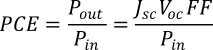
Here, Pout (Pin) is the output (input) power of the cell, FF is the fill factor, and Jsc and Voc are the short-circuit current density and open-circuit voltage respectively.
The short-circuit current density is the photogenerated current density of the cell when there is no applied bias. In this case, only the built-in electric field within the cell is used to drive charge carriers to the electrodes. This metric is affected by:
- Absorption characteristics of the photoactive layer
- Charge generation, transport, and extraction efficiency
The open-circuit voltage is the voltage at which the applied electric field cancels out the built-in electric field. This removes all driving force for the charge carriers, resulting in zero photocurrent generation. This metric is affected by:
- Energy levels of the photoactive materials
- Work functions of the electrode materials
- Charge carrier recombination rate
The fill factor is the ratio of the actual power of the cell to what its power would be if there were no series resistance and infinite shunt resistance. This is ideally as close as possible to 1, and can be calculated using the following equation:
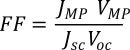
Here, JMP and VMP are the current density and voltage of the cell at maximum power respectively.
Approximate values of the series and shunt resistances can be calculated from the inverse of the gradient of a cell’s JV curve at the Voc and Jsc respectively.
A solar cell is a diode, and therefore the electrical behavior of an ideal device can be modeled using the Shockley diode equation:
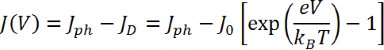
Here, Jph is the photogenerated current density, JD is the diode current density, J0 is the dark saturation current density (current density flowing through the diode under reverse bias in the dark), V is the voltage, and T is the temperature. The final 2 symbols, e and kB, are the elementary charge (1.6 x 10⁻¹⁹ C) and the Boltzmann constant (1.38 x 10⁻²³ m2.kg.s-2.K-1) respectively. However, in reality, no device is ideal and so the equation must be modified to account for potential losses that may arise:
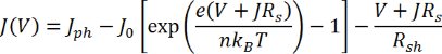
Here, n is the diode ideality factor and all other symbols have their previous meanings. Using this equation, a solar cell can be modeled using an equivalent circuit diagram, which is shown below:

The series resistance (Rs) accounts for resistances that arise from energetic barriers at interfaces and bulk resistances within layers. Ideally, this is minimized to prevent efficiency losses due to increased charge carrier recombination. This can be achieved by ensuring good energy level alignment of the materials used in the solar cell.
The shunt resistance (Rsh) accounts for the existence of alternate current pathways through a photovoltaic cell. Unlike the series resistance, this is ideally as high as possible to prevent current leakage through these alternate paths.
Solar Simulator

Types of Solar Cells
There are several types of solar cells, which are typically categorized into three generations. The first generation (known as conventional devices) are based upon crystalline silicon, a well-studied inorganic semiconductor. The second generation are the thin-film devices, which includes materials that can create efficient devices with thin films (nanometer to tens of micrometers range). The third generation are the emerging photovoltaics - technologies which are still undergoing research to reach commercialization.
The first and second generations contain the most-studied photovoltaic materials: silicon, gallium arsenide, cadmium telluride, and copper indium gallium selenide. These materials are all inorganic semiconductors, and generally work in the most direct manner: a photon is absorbed - creating an exciton, which is thermally dissociated (inorganic semiconductors typically have high dielectric constants) and subsequently transported to the electrodes via an electric field.
First Generation
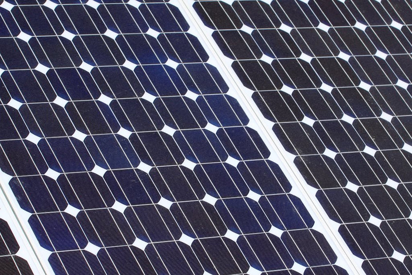
As silicon is the most-studied material, it can achieve some of the highest performances (with a peak efficiency of 26.1%) and was the first material to reach the commercial market. As such, the majority of solar panels use silicon as the photoactive material. The band gap of silicon is 1.1 eV, enabling broad absorption of solar radiation. However, this is lower than the optimum band gap (1.34 eV), resulting in energy losses when absorbing high energy photons. In addition, the band gap is indirect - reducing the absorption efficiency and thus requiring relatively thick layers to efficiently harvest sunlight. As with all inorganic materials, silicon has a high dielectric constant of 11.7 - allowing for the thermal separation of charge-carriers after generation.
Second Generation
Gallium Arsenide
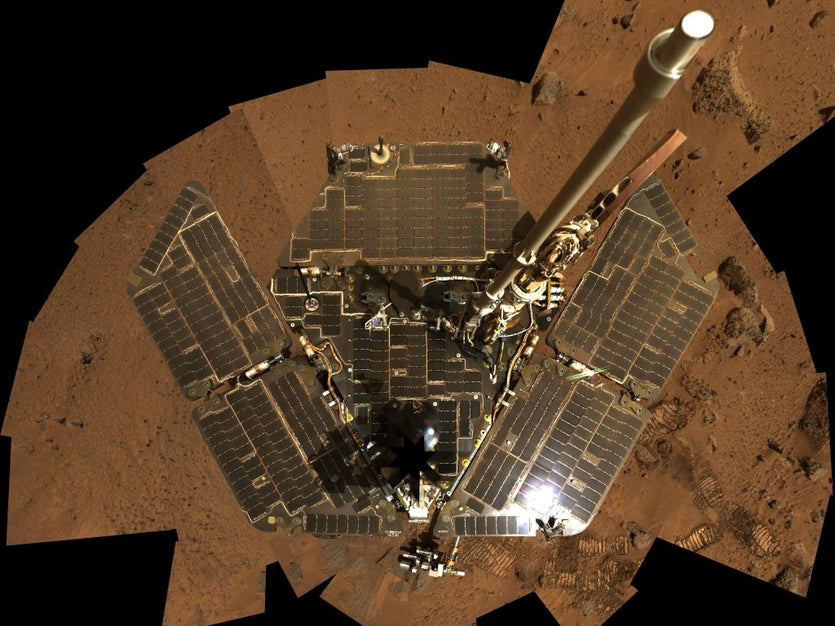
Gallium arsenide (GaAs) boasts the highest performance of any photovoltaic material, reaching 29.1%. This is because GaAs has a direct and more favorable band gap of 1.43 eV - resulting in improved absorption with thinner layers and reduced energy loss. Additionally, GaAs has superior electron-transport properties to silicon. However, it is very expensive to produce as it requires high material purity, which generally limits it to space-based applications (such as satellites and rovers).
Cadmium Telluride
Cadmium telluride (CdTe) is a high-efficiency thin-film photovoltaic technology which has achieved an efficiency of 22.1%. CdTe has a similar band gap to GaAs at 1.44 eV, giving it the same advantages as seen in GaAs - good absorption in thin films and low photon energy losses. This material also boasts the possibility to be flexible, very low costs, and it has produced commercial solar panels that are cheaper than silicon with much shorter energy payback times (although with lower efficiency). Despite these advantages, there are some issues - cadmium is highly toxic and tellurium is very rare, making the long-term viability of this technology uncertain for now.
Copper Indium Gallium Selenide
Copper indium gallium selenide (CIGS) has achieved similar performances to CdTe devices, with a peak of 23.4%. The compound has the chemical formula CuInxGa(1-x)Se2 where x can take a value between 0 and 1. This tunability of the chemical structure enables the band gap of the material to be varied between 1.0 eV (x = 1, pure copper indium selenide) and 1.7 eV (x = 0, pure copper gallium selenide). However, like GaAs cells, CIGS are expensive to fabricate and result in solar panels that cannot compete with the current commercial technologies. Furthermore, like tellurium, indium is very rare, limiting the long-term potential of this technology.
Third Generation
The third generation of photovoltaics - also known as the emerging photovoltaic technologies - includes dye-sensitized, organic, and perovskite solar cells. These materials can degrade when exposed to the environment, negatively affecting the performance and longevity of the solar cell. Glove boxes provide an inert atmosphere to prevent degradation.
Dye-Sensitized

Dye-sensitized solar cells (DSSCs) use organic dyes to absorb light. These dyes are coated onto an oxide scaffold (typically titanium oxide) which are immersed in a liquid electrolyte. The dyes absorb the light, and the excited electron is transferred to the oxide scaffold, whilst the hole is transferred to the electrolyte. The charge carriers can then be collected at the electrodes. These cells are less efficient than inorganic devices, but have the potential to be much cheaper, produced via roll-to-roll printing, semi-flexible, and semi-transparent. However, issues still exist with use of a liquid electrolyte due to temperature stability (as it can potentially freeze or expand), the use of expensive materials, and volatile organic compounds.
Organic
Organic solar cells (OSCs) use organic semiconducting polymers or small molecules as the photoactive materials. To date, efficiencies of 18.2% have been achieved by this technology. These cells work similarly to inorganic devices. However, organic semiconductors generally have low dielectric constants, meaning that the generated exciton cannot be thermally dissociated. Instead, the exciton must be transported to an interface with a material that has an energy level offset greater than the binding energy of the photon. Here, the electron (or hole) can transfer to the other material and split the exciton, allowing the charge carriers to be collected (as shown earlier in the general theory section). As excitons can typically only diffuse approximately 10 nm before the electron and hole recombine, this limits the thickness, structure, and ultimately - the performance of an organic photovoltaic cell. Despite this, these devices hold some significant advantages over inorganic devices, including: low cost of materials, lightweight, strong and tuneable absorption characteristics, flexibility, and the potential to be fabricated using roll-to-roll printing techniques. Currently, organic materials suffer from stability issues arising from photochemical degradation.
Perovskite
Perovskite solar cells (PSCs) use perovskite materials (materials with the crystal structure ABX3) as their light-absorbing layer. Perovskites were introduced to the field relatively recently, with the first use in a photovoltaic device reported in 2006 (where it was the dye in a DSSC achieving 2.2%). However, 2012 is considered the birth of the field, due to the publication of a landmark paper in which an efficiency of 10.9% was achieved. Since then the peak efficiency has risen to 25.5%, making PSCs the fastest-improving solar technology. These materials have remarkable properties, including strong tuneable absorption characteristics and ambipolar charge transport. They can also be processed from solution in ambient conditions.
There are still issues with stability and the use of toxic materials (such as lead) preventing the technology from being commercialized, but the field is still relatively young and very active. For more detailed information about perovskites, see our perovskite guide.
Best Solar Cell Efficiencies
The table below shows the best research cell efficiencies for a variety of photovoltaic technologies (values courtesy of the National Renewable Energy Laboratory, Golden, CO).
| Solar Cell Type | Highest Efficiency (Last updated 09/03/2026) |
|---|---|
| Monocrystalline silicon (mono-Si) | 26.6 % |
| Polycrystalline silicon (multi-Si) | 23.3 % |
| Silicon Heterostructures (HIT) | 27.9 % |
| Amorphous silicon (a-Si) | 14.0 % |
| Monocrystalline gallium arsenide (GaAs) | 27.8 % |
| Cadmium telluride (CdTe) | 23.1 % |
| Copper indium gallium selenide (CIGS) | 23.6 % |
| Dye-sensitized (DSSC) | 13.0 % |
| Organic (OSC / OPV) | 19.4 % |
| Perovskite (PSC) | 27.3 % |

Learn More
 Organic Photovoltaics: An Introduction
Organic photovoltaics (OPVs) have become widely recognized for their many promising qualities. This page introduces the topic of OPVs, how they work and their development.
Read more... Setting Up A Solar Cell Research Lab
To establish a solar cell research lab, you have to consider two main stages. You will need equipment and supplies for both: A solar cell fabrication lab and a solar cell testing lab.
Read more...
References
- World energy outlook and state of renewable energy:..., O. Yolcan (2023)
- Solar energy: Potential and future prospects, E. Kabir et al. (2018)
Further Reading
- A review of solar photovoltaic technologies. Bhubaneswari Parida, Renewable and Sustainable Energy Reviews, Vol 15, p1625-1636 (2011)
- A review of thin film solar cell technologies and challenges. Taesoo D. Lee, Renewable and Sustainable Energy Reviews, Vol 70, p1286-1297 (2017)
- Dye-Sensitized Solar Cells. Anders Hagfeldt, Chemical Reviews, Vol 110, p6595-6663 (2010)