How Do Semiconductors Work?
Jump to: Semiconductor Requirements | Properties of Semiconductors | Types of Semiconductor | What is a p-n Junction? | Traditional Semiconductor: Silicon
Semiconductors are materials with properties that fall between a good conductor (like metals) and a good insulator (like rubber). Depending on the conditions, semiconductors can be conductive or insulating. This ability to control the flow of electrical current is crucial for many modern electrical devices, such as microchips and photovoltaics.
Semiconductor Requirements
For a semiconductor to manipulate electricity in a device, two requirements must be met:
- Charge carrier imbalance - there must be a variation in carrier (electrons (negative charge) or holes (positive charge, representing the absence of an electron)) concentration across the material.
- Charge carrier mobility - under certain conditions, such as an applied electric field, thermal excitation or photon absorption, electrons in the conduction band and holes in the valence band must be able to move through the material with the required mobility for the desired application.
There are different ways charge can be conducted through a semiconductor. The mechanism is dependent on the material itself. Typical semiconducting materials, such as silicon, are solid state lattices of one element that can be modified to incorporate different atoms. Charge flows through the crystalline lattice of that material with different atoms incorporating more of a particular type of charge carrier (electron or hole). Other materials such as small organic molecule do not form lattices. Charge flows within the molecule and also hops between molecules. Whilst this might limit conductivity to some extent these materials offer more opportunities within an electronic device that traditional inorganic semiconductor materials can not.
Charge Transport in Different Semiconductor Classes
Inorganic crystalline semiconductors
Elemental semiconductors such as silicon and compound semiconductors such as gallium arsenide (GaAs) or metal oxides such as zinc oxide (ZnO) consist of a periodic atomic lattice that supports band conduction. In their intrinsic state, these materials exhibit low carrier concentrations, but controlled introduction of dopants (n-type or p-type) generates additional free electrons or holes by creating donor or acceptor energy levels within the band gap. The resulting carrier concentration and mobility are governed by the material’s band structure, effective mass of the carriers, and scattering mechanisms (phonon, impurity, and defect scattering).
Organic Semiconductors
Organic semiconductors, such as small molecules or polymers, generally lack the long-range crystalline order of inorganics, although some (e.g., pentacene) form polycrystalline domains with limited band transport. In many cases, charge conduction is dominated by hopping transport between localized molecular orbitals (HOMO and LUMO). Charge can move both within conjugated molecular backbones (intra-molecular transport) and between adjacent molecules (inter-molecular hopping). While mobilities in these materials are typically lower than in inorganic semiconductors, they offer distinct advantages such as solution processability, mechanical flexibility, low-temperature fabrication, and chemically tunable optoelectronic properties.
Properties of Semiconductors
To understand how semiconductors work, you must understand the fundamental properties of solids.
Electrons that are tied to an atom in an an inorganic solid are confined to energy bands. The valence band is occupied by electrons when the temperature of the solid is absolute zero. In this band, electrons are tightly bound to parent atoms through strong covalent or ionic bonds, making it difficult for them to move freely. The conduction band, on the other hand, contains electrons that gain sufficient energy to break free from the bonds to move more freely. The energy gap between the valence and the conduction band is known as the band gap. The band gap of a material determines many of the optical and electronic properties.
Insulators
Insulators, such as rubber, have a very large band gap, usually greater than 4 eV. A large amount of energy is needed for electrons to move from the valence band to the conduction band. This is unlikely to happen at room temperature, so these materials will not conduct heat or electricity.
Semiconductors
The band gap of semiconductors lies in-between that of conductors and insulators, usually in the range of 0.5-3 eV. It is large enough so that electrons do not ordinarily flow freely through the material. However, when excited by external factors like heat or light, some of the valence electrons gain enough energy to jump to the conduction band, creating holes in the valence band. The creation of free electrons and holes is very important for many applications, including photovoltaics, LEDs, and transistors.
Conductors
In conductors, the valence and conduction bands overlap, so there is effectively no band gap. Electrons require little to no additional energy to move freely through the material, resulting in a high density of charge carriers. Depending on the band structure, these carriers may be electrons or holes. This abundance of mobile carriers allows conductors to efficiently transport both electrical current and thermal energy.

The conduction and valence band structure is the same for all inorganic materials including metal oxide semiconductors. In metal oxide semiconductors, the conduction band minimum (CBM) is mainly formed from metal ns orbitals, while the valence band maximum (VBM) is dominated by oxygen 2p orbitals, with some hybridization between them. The dispersive nature of metal ns orbitals gives electrons a small effective mass and high mobility, whereas localized oxygen 2p orbitals result in holes having a larger effective mass and lower mobility. Consequently, electrons typically move much more easily than holes in these materials.
Examples of Metal Oxide Semiconducting Materials


For semiconducting organic molecules and polymers the energy levels are referred to as the highest occupied molecular orbital (HOMO) and lowest unoccupied molecular orbital (LUMO). They are comparable to the conduction band and the valence band. Semiconducting organic molecules are made up of atomic orbitals that come together to form molecular orbitals. This is where the electrons of the molecule exist or are likely to be found.
In the same way as the conduction and valence band, electrons that exist in the HOMO can be excited to the LUMO. The gap between the HOMO and LUMO is also referred to as the band gap. The advantage of organic molecules over tradition solid state semiconductors is that the HOMO and LUMO can be easily modified to change its electronic and therefore semiconducting properties. This makes them exciting materials to add to electronic devices.
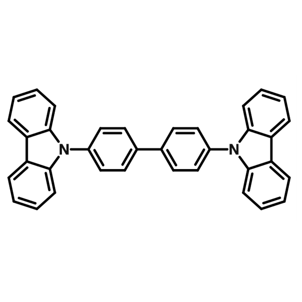
Examples of Organic Semiconducting Materials


Inorganic semiconductors remain dominant in high-speed, high-power, and high-reliability applications due to their high mobilities and well-understood manufacturing processes. Organic semiconductors, despite lower mobilities, enable new classes of devices, such as flexible displays, printed electronics, and bio-integrated sensors. Mechanical compliance, large-area processing, and custom molecular design are more important for these applications than ultimate carrier speed.
Types of Semiconductor
N-type Semiconductors
N-type stands for ‘negative’ due to the extra electrons.
N-type inorganic semiconductors are typically doped crystals (e.g., silicon or germanium with Group V elements) that introduce extra electrons as majority carriers, shifting the Fermi level closer to the conduction band and increasing conductivity. N-type organic semiconductors, by contrast, rely on π-conjugated molecular structures or electron-donating dopants to promote electron transport via the LUMO, with electrons again serving as majority carriers. While inorganic n-types are generally stable, many organic n-types suffer from air instability, requiring protective design or encapsulation.
P-type Semiconductors
P-type stands for ‘positive’ to remind us that this material has more holes.
P-type inorganic semiconductors are typically doped with Group III elements (e.g., boron, aluminum, or gallium) that create electron deficiencies, or holes, as majority carriers, shifting the Fermi level closer to the valence band. P-type organic semiconductors use π-conjugated molecular structures or electron-accepting dopants to facilitate hole transport via the HOMO, with holes serving as the primary carriers and electrons as the minority carriers. While inorganic p-types are generally stable, many organic p-types are more robust in air than their n-type counterparts, though stability can still depend on molecular design and processing.
What is a p-n Junction?
A p-n junction is the most basic kind of semiconductor device. N-type and p-type semiconductors are joined to create a p-n junction diode. One side is more negative and the other is more positive, creating a charge imbalance across the device. The mid-point where the semiconductors meet is the junction. Electrons can move across the junction to the positive side of the diode leaving behind a positively charged donor ion. Holes from the p-type semiconductor do the opposite, leaving behind a negative acceptor ion. This process continues back and forth until the number of electrons which have crossed the junction have a large enough electrical charge to repel or prevent any more charge carriers from crossing over the junction. This creates a neutrally charged area at the junction called the depletion layer as the donor atoms repel the holes and the acceptor atoms repel the electrons.

The size of the depletion zone affects how easy or difficult it is for electrons to move through the semiconductor. When a voltage is applied, the depletion region will decrease enabling electrons to flow in a single direction. If the potential difference is reversed, the depletion zone becomes wider, making it more difficult for electrons to cross the junction. This is known as reverse bias. It acts as a one-way switch, which is useful in devices such as transistors.
Transistors
Transistors are fundamental components of modern electronics. They are made from three connected semiconductor regions. Common materials include silicon, germanium, and compound semiconductors like gallium arsenide. Other types use metal oxides such as zinc oxide or indium gallium zinc oxide, or organic molecules in organic thin-film transistors (OTFTs).
Transistors function as switches or amplifiers. They control the flow of electrical current or increase its strength. You can find them in telecommunications systems, computer memory, and multimedia storage devices.
Metal oxides are often chosen for their transparency and stability, making them useful in displays and flexible electronics. Organic materials are valued for their low-cost fabrication and mechanical flexibility, which suit them to lightweight, bendable devices.
Traditional Semiconductor: Silicon
Silicon is commonly used in semiconductor devices. However, naturally occurring silicon is electrically inert. Sitting between carbon and germanium on the periodic table, these elements have much in common. Each have four electrons in their outer orbital shells which can form covalent bonds with the outer shell electrons of surrounding atoms. As a result, they can form a crystalline structure.
Despite the metallic appearance of silicon crystals, they are not metals. Like their carbonic counterparts, they are very stable. In fact, the lack of free moving electrons within this material renders it more like an insulator than a metal.
Other materials can be added to increase the electrical potentiality of silicon. In a process called doping, impurities are introduced to the material to alter its physicochemical properties. These impurities are often atoms with either 3 or 5 electrons in their valence band. The imbalance created allows for the free movement of electrons within the material. There are two ways of doping silicon: n-type doping, and p-type doping.
N-type doping
Impurities with five electrons (pentavalent) in their outer shell are added to the silicon crystal structure. This results in an unbound ‘free’ electron.
P-type doping
Impurities with three electrons (trivalent) in their outer shell are added to the silicon crystal structure. Three of the electrons can bond with silicon outer shell electrons leaving a ‘hole’. These spare holes enable electrical conductivity in the materials as they are able to accept free moving electrons once a current is flowing.
Semiconducting Molecules
Learn More
 What are Organic Semiconductors?
Organic semiconductors are materials, ranging from small molecules to polymers, that can transport charge. Unlike in conductors, where electrons move freely across the material, organic semiconductors rely on a structure primarily composed of carbon and hydrogen atoms.
Read more... What is an n-Type Semiconductor?
An n-type semiconductor is a type of semiconductor where electrons serve as the majority charge carriers, leading to a negative charge transport characteristic. These electron-donating properties make n-type semiconductors suitable for electrical applications, particularly in transistors, LEDs, solar cells and electrodes.
Read more...Contributing Authors
Written by
Professional Science Writer
Reviewed and edited by
Application Scientist
Edited by
Application Scientist