
Perovskites and Perovskite Solar Cells: An Introduction

The rapid improvement of perovskite solar cells has made them the rising star of the photovoltaics world and of huge interest to the academic community. Since their operational methods are still relatively new, there is great opportunity for further research into the basic physics and chemistry around perovskites. Furthermore, as has been shown over the past few years, the improvements of perovskite materials and fabrication routines, using a glove box, has led to significant increases in power conversion efficiency, with recent devices reaching 26.7% as of 2025. They also achieved up to 30.1% for perovskite/perovskite tandem solar cells and 34.6% for perovskite/silicon tandem solar cells.1
What are Perovskites?
The terms "perovskite" and "perovskite structure" are often used interchangeably. Technically, a perovskite is a type of mineral that was first found in the Ural Mountains and named after Lev Perovski (who was the founder of the Russian Geographical Society). A perovskite structure is any compound that has the same structure as the perovskite mineral.True perovskite (the mineral) is composed of calcium, titanium and oxygen in the form CaTiO3.
More generally, a perovskite structure is anything that has the generic form ABX3 and the same crystallographic structure as perovskite (the mineral). However, since most people in the solar cell world aren’t involved with minerals and geology, perovskite and perovskite structure are used interchangeably.
The perovskite unit cell is demonstrated below. As with many structures in crystallography, it can be represented in multiple ways. The simplest way to think about a perovskite is as a large atomic or molecular cation (positively-charged) of type A in the centre of a cube. The corners of the cube are then occupied by atoms represented by B (also positively-charged cations) and the faces of the cube are occupied by a smaller atom X with negative charge (anion).

Depending on which atoms/molecules are used in the structure, perovskites can have an impressive array of interesting properties, including superconductivity, giant magnetoresistance, spin-dependent transport (spintronics) and catalytic properties. Perovskites therefore represent an exciting playground for physicists, chemists and material scientists.
Perovskites were first successfully used in solid-state solar cells in 2012,2,3 and since then most cells have used the following combination of materials in the usual perovskite form ABX3:
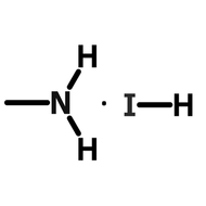
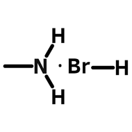
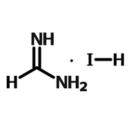
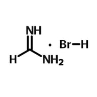
- A = An organic cation - methylammonium (CH3NH3+) or formamidinium (NH2CHNH2+)
- B = A big inorganic cation - usually lead(II) (Pb2+)
- X3= A slightly smaller halogen anion – usually iodide (I-), bromide (Br-) or chloride (Cl-)
Since this is a relatively general structure, these perovskite-based devices can also be given a number of different names, which can either refer to a more general class of materials or a specific combination. As an example of this, we’ve created the table below to highlight how many names can be formed from one basic structure.
| A | B | X3 |
| Organo | Metal | Trihalide (or trihalide) |
| Methylammonium | Lead | Iodide (or triiodide) |
| Mixed-cation (also triple cation or double cation) | Plumbate | Chloride (or trichloride) |
The table demonstrates how vast the parameter space is for potential material/structure combinations, as there are many other atoms/molecules that could be substituted for each column. The choice of material combinations will be crucial for determining both the optical and electronic properties (e.g. bandgap and commensurate absorption spectra, mobility, diffusion lengths, etc). A simple brute-force optimisation by combinatorial screening in the lab is likely to be very inefficient at finding good perovskite structures.
The majority of efficient perovskites are based on Group IV (specifically, lead) metal halides, and moving beyond this has proved challenging. It is likely more in-depth knowledge than currently available is required to fully explore the range of possible perovskite structures. Lead-based perovskite-based solar cells are particularly good because of a range of factors, including strong absorption in the visible regime, long charge-carrier diffusion lengths, a tuneable band gap, and easy manufacture (due to the high defect tolerance and the ability to process at low temperatures).
When solution processing perovskite films, perovskite precursor materials, are dissolved into a perovskite ink. These inks often consist of an organic-halogen salt (MAI, FAI, etc) combined with an inorganic salt (usually lead iodide or lead bromide) in a polar solvent.
Example Perovskite Materials
Why are Perovskite Solar Cells So Significant?
There are two key graphs which demonstrate why perovskite solar cells have attracted such prominent attention in the short time since 2012. The first of these graphs (which uses data taken from the NREL solar cell efficiency chart)1 demonstrates the power conversion efficiencies of the perovskite-based devices over recent years, in comparison to emergent photovoltaic research technology, and also traditional thin-film photovoltaics.
The graph shows a meteoric rise compared to most other technologies over a relatively short period of time. Within 4 years of their breakthrough, perovskite solar cells had equalled efficiencies of Cadmium Telluride (CdTe), which has been around for over 40 years. Furthermore, as of June 2018 they have now exceeded all other thin-film, non-concentrator technologies - including CdTe and Copper Indium Gallium Selenide (CIGS). Although it could be argued that more resources and better infrastructure for solar cell research have been available in the last few years, the dramatic rise in perovskite solar cell efficiency is still incredibly significant and impressive.

The second key graph below is the open-circuit voltage compared to the band gap for a range of technologies that compete against perovskites. This graph demonstrates how much of a photon’s energy is lost in the conversion process from light to electricity. For standard excitonic-based, organic-based solar cells, this loss can be as high as 50% of the absorbed energy, whereas perovskite solar cells regularly exceed 70% photon energy utilisation, and have the potential to be increased even further.4
This is approaching the values of state-of-the-art technologies (such as GaAs), but at a significantly lower cost. Crystalline silicon solar cells, arguably the closest comparator to perovskites in terms of efficiency and cost, are already up to 1000 times cheaper than state-of-the-art GaAs.5 Perovskites have the potential to become even cheaper than this.

Another benefit of perovskite solar cells is that they can be easily deposited, adapted and optimized via solution processing. The easiest and most efficient way of depositing perovskite thin films is to dissolve the precursors in a solution, then coat your substrate using your chosen thin film coating method. Perovskites solar cells fabrication methods are often compatible with roll to roll processing (R2R processing) methods, currently used in large scale manufacturing. Examples of these methods include slot-die coating or inkjet printing. This is a very interesting prospect, especially related to PSC scalability and potential commercialisation.
Many perovskite materials can also be processed at relatively low temperatures (>150 °C). These properties allow you to construct perovskite solar cells on a wide range of substrates, including on flexible or curved substrates.
What Issues Do Perovskites Face?
The biggest issue in the field of perovskites currently is long-term instability. This has been shown to be due to degradation pathways involving external factors, such as water, light, and oxygen,7 and also as a result of intrinsic instability, such as degradation upon heating, because of the properties of the material.4
Several strategies have been proposed in order to improve stability, most successfully by changing component choice. Using mixed-cation systems (for example by including inorganic cations such as rubidium or caesium) has been shown to improve both stability and efficiency.8 The first perovskite cells to exceed 20% efficiency used a mixed organic cation system,9 and many of the highest-efficiency systems published recently use inorganic components. Movement towards hydrophobic, UV-stable interfacial layers has also improved stability – for example by replacing TiO2, which is susceptible to UV degradation, with SnO2.10
Stability has also been improved through use of surface passivation11 and by combining 2D-layered (Ruddlesden-Popper) perovskites (which show better intrinsic stability, but poorer performance) with conventional 3D perovskites.12 These efforts (along with factors such as better encapsulation)13 have vastly improved the stability of perovskites since their initial introduction, and lifetimes are well on their way to meeting industrial standards – with recent work showing cells able to withstand a 1000-hour damp heat test.14

Another issue yet to be fully addressed is the use of lead in perovskite compounds. Though it is used in much smaller quantities than those currently present in either lead- or cadmium-based batteries, the presence of lead in products for commercial use is problematic. Concerns still remain about exposure to toxic lead compounds (through leaching of the perovskite into the environment), and some studies have suggested large-scale implementation of perovskites would require complete containment of degradation products.15 In contrast, other life cycle assessments have found the toxicity impact of lead to be negligible in comparison to other materials in the cell (such as the cathode).5
There is also potential for a lead alternative to be used in perovskite solar cells (such as tin-based perovskites), but the power conversion efficiency of such devices is still significantly behind lead-based devices, with the record for a tin-based perovskite currently standing at 9.0%.16 Some studies have also concluded that tin may actually have a higher environmental toxicity than lead,17 and other less toxic alternatives are required.
Another major issue in terms of performance is the current-voltage hysteresis commonly seen in devices. The factors impacting hysteresis are still under debate, but it is most commonly attributed to mobile ion migration in combination with high levels of recombination.18 Methods to reduce hysteresis include varying cell architecture, surface passivation, and increasing lead iodide content,19 as well as general strategies to reduce recombination.

To enable a truly low cost-per-watt, perovskite solar cells need to have achieved the much-heralded trio of high efficiency, long lifetimes, and low manufacturing costs. This has not yet been achieved for other thin-film technologies, but perovskite-based devices currently demonstrate enormous potential for achieving this.
Fabrication and Measurement of Perovskite Solar Cells
Although perovskites come from a seemingly different world of crystallography, they can be incorporated very easily into a standard OPV (or other thin-film) architecture. The first perovskite solar cells were based on solid state dye-sensitised solar cells (DSSCs), and so used a mesoporous TiO2 scaffold. Many cells since have followed this template or used an Al2O3 scaffold in a ‘meso-superstructured’ architecture, but the high temperature steps required for manufacture, and UV instability of TiO2, led to introduction of a ‘planar’ architecture similar to other thin-film cells. After several years of lagging behind mesoporous cells in terms of efficiency, planar perovskites are now almost as efficient.20

The perovskite film itself is typically processed by either vacuum or solution methods. Film quality is very important. Initially, vacuum-deposited films gave the best devices, but this process requires the co-evaporation of the organic (methylammonium) component at the same time as the inorganic (lead halide) components, necessitating specialist evaporation chambers that are not available to many researchers. As a result, there have been significant efforts into improving solution-processed devices, as these are simpler and allow for low-temperature processing, and these now equal vacuum-deposited cells in terms of efficiency.21
Typically, the active layer of a perovskite solar cell is deposited via either a one or two-step process. In the one-step process, a precursor solution (such as a mix of CH3NH3I and PbI2) is coated that then converts to the perovskite film upon heating. A variation on this is the ‘antisolvent’ method, in which the precursor solution is coated in a polar solvent, and then quenched during the spin coating process by a non-polar solvent. Precise timings of the quench and volumes of the quenching solvents is required to give the optimal performance.
In the two-step process, the metal halide (such as PbI2) and organic components (such as CH3NH3I) are spin-coated in separate, subsequent films. Alternatively, metal halide films can be coated and annealed in a chamber filled with the organic component vapour, known as ‘vacuum-assisted solution process’ (VASP).22

Most state-of-the-art perovskites are based on a transparent conducting oxide/ETL/Perovskite/HTL/metal structure, where ETL and HTL refer to electron-transport and hole-transport layers respectively. Typical hole-transport layers include Spiro-OMeTAD or PEDOT:PSS, and typical electron-transport layers include TiO2 or SnO2. Understanding and optimising the energy levels and interactions of different materials at these interfaces offers a very exciting area of research that is still under discussion.
The main issues for practical device fabrication of perovskite solar cells are film quality and thickness. The light-harvesting (active) perovskite layer needs to be several hundred nanometres thick – several times more than for standard organic photovoltaics, and creating such thick layers with high uniformity can be difficult. Unless the deposition conditions and annealing temperature are optimised, rough surfaces with incomplete coverage will form. Even with good optimisation, there will still be a significant surface roughness remaining. Therefore, thicker interface layers than might normally be used are also required. Improvements to film quality have been achieved through a variety of methods. One such method is the addition of small amounts of acids, such as hydroiodic or hydrobromic acid or excess of lead iodide precursor.19
Through extensive research efforts, efficiencies of over 22% have been achieved using spin coating,23 and high efficiencies have also been achieved using other solution-processing techniques.24 This suggests that large-scale solution processing of perovskites is very feasible.
The Future of Perovskites
Future research into perovskites is likely to focus on the reduction of recombination through strategies such as passivation and reduction of defects, as well as boosting efficiency through inclusion of 2D perovskites and better-optimised interface materials. Charge-extraction layers are likely to move away from organic materials to inorganic, to improve both efficiency and stability. Improving stability and reduction in the environmental impact of lead are likely to both continue to be significant areas of interest.
Whilst the commercialisation of standalone perovskite solar cells still faces obstacles in terms of fabrication and stability, their use in tandem c-Si/perovskite cells has progressed rapidly (with efficiencies above 25% achieved)25 and it is likely that perovskites will first see the PV market as part of this structure. Beyond solar, there remains significant potential for use of perovskites in other applications, such as light-emitting diodes26 and resistive memories.27
Perovskite Materials

Keep Reading...
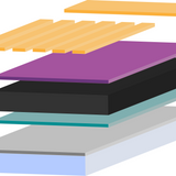 Perovskite Solar Cell Layers
Perovskite solar cells need several layers to effectively separate and extract charge. There are several materials you can use as absorbers and transport layers.
Read more... Perovskite Solar Cells: Causes of Degradation
One of the major challenges in the development of perovskite solar cells is the improvement of their stability and durability. A range of extrinsic and intrinsic factors can lead to device degradation.
Read more...References
- NREL’s ‘Best Research-Cell Efficiencies’. Available at: https://www.nrel.gov/pv/assets/pdfs/pv-efficiencies-07-17-2018.pdf. (Accessed: 14th December 2018)
- Efficient Hybrid Solar Cells Based on Meso-Superstructured Organometal Halide Perovskites., M. M. Lee et al., Science, Vol. 338, p643–647 (2012).
- Lead iodide perovskite sensitized all-solid-state submicron thin film mesoscopic solar cell with efficiency exceeding 9%., H.-S. Kim et al., Scientific Reports, Vol 2 (2012).