Source-Drain Deposition Mask, High Density
Substrates and Fabrication
For High Quality deposition of source-drain contacts
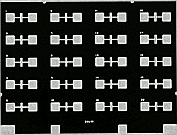
Produce 20 OFETs on a single substrate
Overview | Specifications | Resources
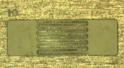
Shadow masks for deposition of source-drain contacts. Designed for use in the Evaporation Stack for High Density OFETs with our standard sized substrates of 20 x 15 mm. Each mask produces 20 OFETs on a single substrate. We sell a selection of masks for different precisions in linear and interdigitated patterns.
If you would like to mix and match geometries, please contact us.
General Mask Specifications
| Mask dimensions | 20 x 15 mm |
| Number of OFETs | 20 |
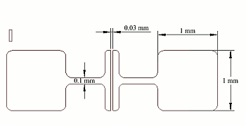
| Contact pad size | 1 mm x 1 mm |
| Contact pitch | 2.54 mm (0.1") |
| Mask material | Electroformed nickel |
| Compatible products |
Individual Mask Specifications
| Product Code | E321 | E322 | E323 |
|---|---|---|---|
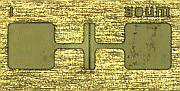
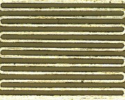
| Channel Geometry | Linear | Linear | Interdigitated |
| Channel Width | 1 mm | 1 mm | 18.23 mm |
| Channel Length | 30 µm | 30, 40, 50, 60, 80 µm (4 of each) | 50 µm |
| Tolerance | ± 7 µm | ± 7 µm | ± 7 µm |
| Mask Thickness | 30 µm | 30 µm | 30 µm |
Linear 1 mm x 30 µm (E321) and 1 mm x 30 µm variable (E322)
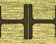
Interdigitated 18 mm x 50 µm (E323)
Troubleshooting
The mask is designed in such a way that during the deposition of the gate electrodes on the corner of the substrate the metal should cover the edge of the substrate as well. This ensures conductivity between the metal electrodes and the p-doped silicon. If you find the edges of the substrate not to be conductive you must scratch the edges of the substrate to remove the insulating silicon oxide in correspondence with the corner where the gate electrode will be deposited.

B-Grade Masks
Masks with one channel that falls outside of our quality standards are listed as B-Grade. The other 19 channels on these masks are of the same standard as on our A-Grade masks. It is possible that the substandard channel may produce a working device, however this cannot be guaranteed. Therefore, these B-Grade masks are offered at a discounted price.