Analyzing and Improving Solar Cell Metrics: FF , VOC and JSC

Device metrics are extracted from current-voltage curves (J-V curves) and are vital in determining how efficiently your device is converting sunlight into electricity. They can also be extremely helpful in diagnosing problems in your device. By analyzing key device metrics such as fill factor (FF), open-circuit voltage (VOC), short-circuit current (JSC), and power conversion efficiency (PCE), you can not only evaluate the effectiveness of your solar cell devices but also diagnose potential issues and identify areas for improvement.
In this article, we will delve into the intricacies of analyzing key device metrics, focusing on how low FF, low VOC and low JSC can hinder device performance. This will help you gain a deeper understanding of the factors influencing solar cell performance and the techniques required to diagnose and improve device efficiency.
Low VOC
VOC represents the maximum voltage across a solar cell when no external load is connected. It directly relates to the energy level alignment within the solar cell and serves as a key parameter to assess the device's ability to generate electrical power in the absence of a load. VOC is ultimately a measure of the quality and band gap of your absorber material and the dominant recombination processes within your device.
Therefore, a low VOC could be a sign of several issues in your device. It could indicate that there may be:
- Trap states in your device
- Impurities or non-photoactive phases in your active layer
- Series and shunt resistance + interfacial dynamics
- Small bandgap
- Mismatched energy band alignment
If your devices suffer from low VOC, a passivating layer could help boost this. Also, to get a high VOC, you need to ensure that you have a high-quality absorber layer. In the case of solution processed solar cells (such as perovskite solar cells or organic solar cells) incomplete conversion of absorber material could lead to non-photoactive phases which can act as trap states for charge carriers.
Low JSC
JSC represents the maximum current that flows through a solar cell when the voltage across it is zero. It provides insights into the ability of the device to capture and utilize the AM1.5 spectrum. JSC can help you quantify the light absorbing capability of your solar cell and optimize the device's structure, materials, and interfaces to enhance current generation. JSC relies heavily on a quality known as the quantum efficiency - which represents what percentage of incoming photons are converted into useful charge carriers. It is also a measure of your solar cell's capacity to effectively separate and extract charge. JSC is therefore affected by light absorption properties within your active layer and charge carrier extraction from it. Surface recombination, bulk defects, and trap-assisted recombination processes can contribute to carrier losses. To achieve a high JSC, you will need consider several factors:
- Smaller band gaps will lead to increased JSC as more electrons will be able to cross the energy barrier. However, this will compromise your VOC.
- You can use an antireflective coating on top of your device to reduce reflection, introduce surface texturing techniques or various interlayers (such as reflective interlayers, photon down- or up-shifting layers or light trapping layers) to improve light harvesting properties of your device.
- Doping the transport layers of your device (such as dopants used for Spiro-OMeTAD) can improve the conductivity of your layers, aiding charge transport.
- Thicker active layers allow more chances for photon absorption, but this also increases the distance the charge carrier must travel before being extracted. If charge transport layers are too thin, this can interrupt charge transport to the contacts for extraction.
- This is the metric that will be most affected by a deviation in solar irradiance. You should therefore check that your solar simulator light source is functioning correctly if the JSC changes gradually over time.
All of these factors should be optimized for your specific device and absorber material if you want to obtain the highest JSC.
Low FF
Fill factor (FF) is determined as the maximum power value divided by the product of VOC and JSC. Fill factor is often defined as a metric that describes the "squareness" of a J-V curve and is related to both series and shunt resistance within your device.
To improve the fill factor of your devices, you must aim to decrease series and shunt resistance, while increasing JSC and VOC. There are many things you can do to improve fill factor:
- Optimize the thickness of your device layers.
- Ensure there are no shunt pathways through your device.
- Do everything you can to reduce defects in your films.
- Examine the energy band alignment of the layers in your device.
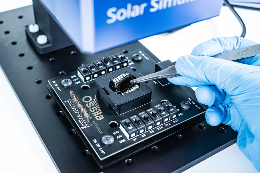
Solar Simulator

Learn More
 I-V Curves: A Guide to Measurement
An I-V curve (short for 'current-voltage characteristic curve'), is a graphical representation of the relationship between the voltage applied across an electrical device and the current flowing through it.
Read more... Fill Factor of Solar Cells
Fill factor (FF) is an important measurement that you can use to evaluate the efficiency of solar cells. To calculate fill factor, you need to divide the maximum possible power output of a cell by its actual power output.
Read more...