Tungsten Diselenide (WSe2) Powder and Crystal
CAS Number 12067-46-8
2D Materials, Low Dimensional Materials, Materials, Transition Metal Chalcogenides (TMCs), Transition Metal Dichalcogenides (TMDs)
Low price, high purity 2D tungsten Diselenide (WSe2) powder and crystals
Suitable for the creation of single or few-layer sheets via mechanical or liquid exfoliation
Technical Data | MSDS | Structure | Literature and Reviews | Related Products | Resources and Support
Bulk tungsten diselenide (WSe2), CAS number 12067-46-8, has a high absorption coefficient, high photostability, and a band-gap of 1.2 eV. It is an indirect band-gap semiconducting material that can be both n- and p-doped. The ambipolar nature of WSe2 makes it possible to create electronic devices that include p−n junctions or complementary logic circuits.
Tungsten diselenide single layers are composed of a layer of tungsten atoms positioned between two layers of selenium atoms, with each tungsten atom coordinating through strong covalent-ionic bonds to six selenium atoms in a trigonal prismatic geometry. As occurs in graphene, black phosphorus, and other TMDC materials, multilayer structures are stabilised by weak Van de Waal forces. These forces are strong enough to hold layers together, but weak enough to allow mechanical exfoliation.
High Purity
≥99.999% Crystal Purity
Worldwide shipping
Quick and reliable shipping
Low Cost
Low Cost Tungsten Diselenide
Powder & Crystal
Different Forms of Tungsten Diselenide
Like WS2 and other TMDCs, 2-dimensional layered tungsten diselenide (WSe2) has a 2H (semiconducting) structure. This structure is the more stable form of the two hexagonal phases that exist in the naturally-occurring bulk-material forms. A 1T octahedral phase also exists - this is metallic in nature and is only associated with single layer films. Monolayer, few-layer nanosheet structures, and nanoparticles can be prepared by mechanical or chemical exfoliation. It has been demonstrated that the phase change from 2H to 1T can happen via chemical treatments, such as lithium-assisted intercalation of bulk crystals or powder by liquid exfoliation.
We supply low price tungsten diselenide in several different forms for a range of applications.
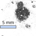
Tungsten Diselenide Powder
Can be used for preparation of tungsten diselenide nanoplates and ultrathin films
Available in quantities of 500 mg or 1 g
≥99.995% purity
From £220
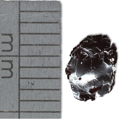
Tungsten Diselenide Crystals by Size
Can be used to produce single or few-layer tungsten diselenide sheets via mechanical or liquid exfoliation
Small (≥10 mm2) or medium (≥25 mm2) crystals available*
≥99.999% purity
From £520
*Typical representative size, areas/dimensions may vary
Bulk single tungsten diselenide crystal is most commonly used as sources from which single or few-layer sheets can be obtained via either mechanical or liquid exfoliation. Single tungsten diselenide crystal or films produced from such crystals are suitable for study using atomic force microscopy or transmission electron microscopy
Few-layer WSe2 nanosheets and nanoparticles can also obtained from tungsten diselenide powder by liquid-exfoliation using mixture of 30% of isopropanol in water. Ti and V intercalated WSe2 create delocalized antiferromagnetism, while Cr, Mn, Fe, and Co exhibit localized ferromagnetism in WSe2. Iron-series transition-metal atoms intercalated WSe2 may have potential applications in spin electronics and quantum-information devices.
Technical Data
| CAS Number | 12067-46-8 |
| Chemical Formula | WSe2 |
| Molecular Weight | 341.76 g/mol |
| Bandgap | 1.4 - 2.01 eV |
| Preparation | Synthetic - Chemical Vapour Transport (CVT) |
| Structure | Hexagonal (2H) |
| Electronic Properties | 2D semiconductor |
| Melting Point | >1200 °C |
| Colour | Metallic black |
| Synonyms | Tungsten selenide, Tungsten(IV) Selenide |
| Classification / Family | Transition metal dichalcogenides (TMDCs), 2D Semiconductor materials, Charge Density Wave (CDW), type II Weyl semimetal, Nano-electronics, Nano-photonics, Photovoltaic, Materials science |
Product Details
| Form | Purity |
|---|---|
| Powder | ≥99.995% |
| Crystal | ≥99.999% |
Pricing Table
| Product Code | Form | Size/Weight* | Price |
|---|---|---|---|
| M2111C1 | Powder | 500 mg | £220 |
| M2111C1 | Powder | 1 g | £350 |
| M2111A10 | Crystal | Small (≥10 mm2) | £520 ea. |
| M2111A25 | Crystal | Medium (≥25 mm2) | £850 ea. |
| M2111A00 | Crystal | Large** (≥100 mm2) | £2300 ea. |
*Typical representative size, areas/dimensions may vary
**Item with a lead time of 4 - 6 weeks, please contact for more information
Shipping is free for qualifying orders.
MSDS Documents
 Tungsten diselenide powder
Structure of Tungsten Diselenide
Tungsten diselenide single layers are composed of a layer of tungsten atoms positioned between two layers of selenium atoms, with each tungsten atom coordinating through strong covalent-ionic bonds to six selenium atoms in a trigonal prismatic geometry. As occurs in graphene, black phosphorus, and other TMDC materials, multilayer structures are stabilised by weak Van de Waal forces. These forces are strong enough to hold layers together, but weak enough to allow mechanical exfoliation.
Like WS2 and other TMDCs, 2-dimensional layered tungsten diselenide (WSe2) has a 2H (semiconducting) structure. This structure is the more stable form of the two hexagonal phases that exist in the naturally-occurring bulk-material forms. A 1T octahedral phase also exists - this is metallic in nature and is only associated with single layer films. Monolayer, few-layer nanosheet structures, and nanoparticles can be prepared by mechanical or chemical exfoliation.
The 2H-WSe2 phase has a hexagonal symmetry, with a trigonal prismatic metal coordination, where layers of selenium atoms are stacked directly above one another. The 1T-WSe2 phase has a tetragonal symmetry, with an octahedral metal coordination, as the layers are offset from each other. It has been demonstrated that the phase change from 2H to 1T can happen via chemical treatments, such as lithium-assisted intercalation of bulk crystals or powder by liquid exfoliation.

Literature and Reviews
- Layer-dependent electronic structure of an atomically heavy two-dimensional dichalcogenide, P-C. Yeh et al., Phys. Rev. B 91, 041407 (2015); DOI: 10.1103/PhysRevB.91.041407.
-
Strain-Induced Indirect to Direct Bandgap Transition in Multilayer WSe2,
S. B. Desai et al., Nano Lett., 14 (8), 4592–4597 (2014); DOI: 10.1021/nl501638a. - Large-Area Synthesis of Highly Crystalline WSe2 Monolayers and Device Applications, J. Huang et al., ACS Nano, 8 (1), 923–930 (2014); DOI: 10.1021/nn405719x.
Related Products
We stock a wide range of 2D materials available to purchase online. Please contact us if you cannot find what you are looking for.