Self-Assembled Monolayers in Electronic Devices

Self-assembled monolayers (SAMs) provide a versatile and cost-effective method for surface modification and the creation of molecular-scale electronic devices. By selecting the appropriate head, spacer and tail group for the SAM molecules the following properties can be adjusted:
- Hydrophobicity
- Hydrophilicity
- Surface energy
- Specific chemical functionality
This versatility is crucial in electronic devices used in surface active applications, where surface properties directly influence device performance. SAMs can form ultra-thin insulating layers that are crucial in constructing nanoscale electronic components. These layers help reduce leakage currents and improve the performance of transistors and other devices.
Also in molecular electronics, SAMs serve as the foundation for constructing devices at the molecular scale. By arranging functional molecules in a controlled manner, it is possible to create molecular diodes, transistors, and other electronic components. The precise control over molecular orientation and spacing provided by SAMs enables the exploration of quantum mechanical effects in electronic devices.
Organic Field-Effect Transistors (OFETs)
Self-assembled monolayers play a significant role in the development of organic field-effect transistors (OFETs). They can be used to modify the interfaces between OFET components; source/drain electrodes, gate dielectric and organic semiconductor. SAMs enhance charge carrier mobility and improving device performance.

Organic Semiconductor / Gate Dielectric interface
SAMs create a well-ordered interface between the organic semiconductor and the gate dielectric. The molecules self-assemble onto the gate dielectric to protect it from unwanted reactions, particularly with moisture. SAMs also improve the morphology of semiconducting layer and grain size. They can also play a role in improving charge transport by reducing the areas of charge immobilization (charge trap sites).
OFET devices with pentacene (organic semiconductor) coated on phosphonic acid (PA) SAM modified Si with a thermally grown oxide layer as a gate dielectric show high charge carrier mobilities up to 4.1 cm2 V−1 s−1.
Gate / Organic Semiconductor interface
SAMs can also act as a nanometer-thick/high-capacitance gate dielectric layer. The reduction of thickness of the dielectric film increases the density of charge carriers in the channel and increases the capacitance of the OFET. SAMs also increase the energy barrier which reduces leakage currents. Overall SAMs can be used to improve device efficiency.
A multilayer approach has also been used which is referred to as self-assembled nanodielectrics (SANDs).
Gate Dielectric / Electrode interface
If the SAM molecule terminal group is π-conjugated it acts as the semiconductor channel. Intermolecular charge transport across the SAM can occur when the device is in a planar configuration. The SAM molecules assemble on the gate dielectric and act as the charge transport layer. In this case the device is called a SAMFET. They have fewer boundaries and defects, and no charge carrier polarization effects from inactive upper layers. In SAMFETs, the conducting channel allows 2D charge transport within its active molecular film, unlike “standard” OFETs, which use thicker OSC films for 3D charge transport.
Electrode / Organic semiconductor interface
SAM functionalization of source and drain electrodes is used for establishing an efficient charge injection between the organic semiconductor and the electrodes. SAMs can simultaneously tune the organic semiconductor morphology, the metal electrode work function and the charge carrier transmission across the injection barrier.
Overall, SAMs play a crucial role in optimizing the performance of FETs by improving interface quality, charge transport, and device efficiency. These advancements highlight the potential of SAMs in the development of high-performance OFETs and related electronic devices.
Light-Emitting Diodes (LEDs)
Self-assembled monolayers can be introduced at various interfaces within the LED device to enhance charge injection and transport. As a result, operating voltage is reduced, and efficiency and stability are improved. ITO modified with nano-scale self-assembled monolayers is known to replace both hole injection and hole transport layers and simplify the device structure.

Self-assembled monolayer modified ITO electrode has improved work function, and ensured effective hole injection to the emitting layer. The most used head groups to modify ITO electrode are:
- Phosphonic acid (PAs)
- Carboxylic acids
- Silanes
PAs are generally preferable to bind to the metal oxide surface. This is because it has more robust interaction forces than carboxylic acids and milder process conditions than silanes.
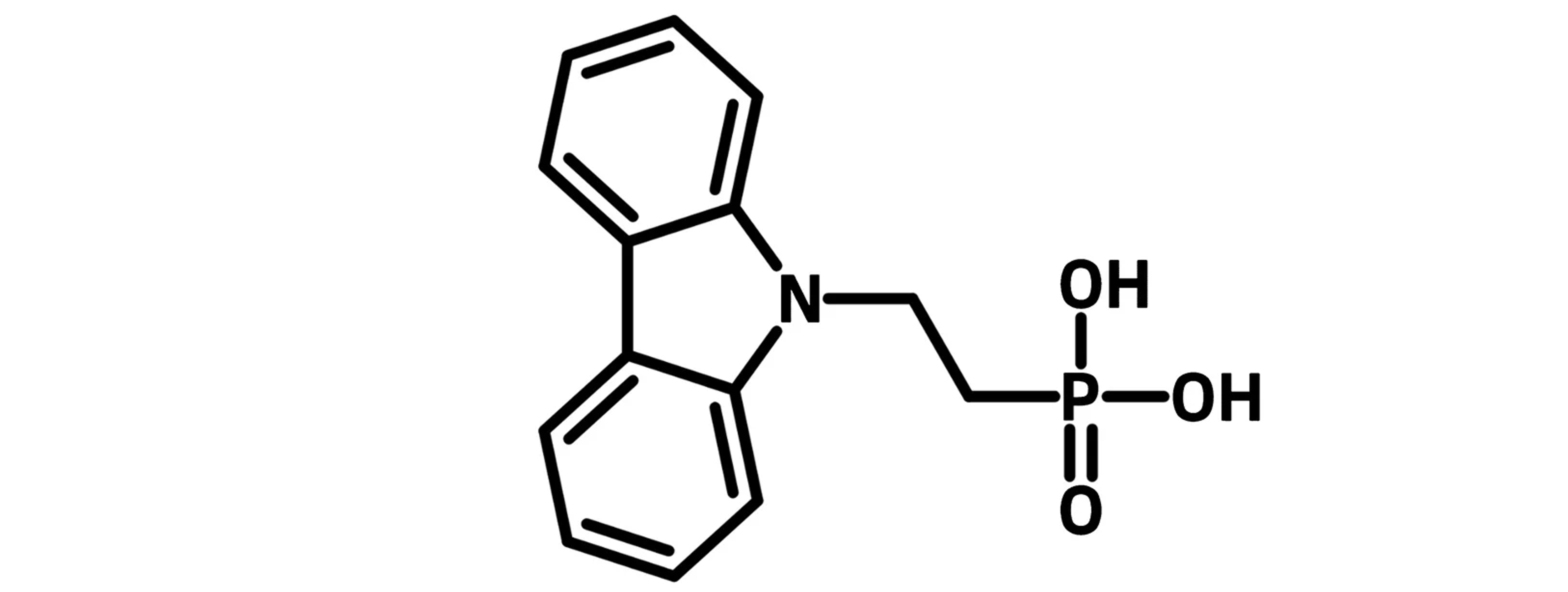
Example SAMs in OFETS include:
Solution-processed phosphorescent OLED with SAM 2,3,4,5,6-pentafluorobenzylphosphonic acid (F5BnPA) functionalized ITO and tris(2-(p-tolyl)pyridine-C2,N)iridium(III) (Ir(mppy)3) green dopant achieved a maximum power efficiency of 63.13 lm W−1 and preferable current efficiency of 60.32 cd A−1. This is the state-of-the-art among the reported solution-processed OLEDs with similar emitters.
HIL/HTL-free green TADF-OLED based on DACT-II:26DCzPPy as the emission layer demonstrated favorable luminescence performance including a current efficiency (CE) of 76.9 cd A–1, and an external quantum efficiency (EQE) of 22.0%.
Polymer Solar Cells (PSCs)
Self-assembled monolayers play a crucial role in enhancing the performance of polymer solar cells (PSCs) by improving various interfacial properties. By choosing appropriate SAM molecules, the work function of the electrode can be adjusted to match the energy levels of the active layer. This facilitates efficient charge injection or extraction. This tuning minimizes energy barriers and reduces losses at the interfaces.
The molecules in SAMs often possess dipole moments that can create an electric field at the interface. This field can shift the energy levels of the electrode, aligning them more closely with the energy levels of the donor and acceptor materials in the polymer blend.

Defect Passivation
SAMs passivate surface states and defects at the electrode interface, which are common sites for charge recombination. By reducing defects at these recombination sites, SAMs enhance the charge collection efficiency. The ordered structure of SAMs can facilitate more efficient charge transport across the interface, reducing resistance and improving overall device performance.
Modified Surface Energy
SAMs can also modify the surface energy of electrodes, making them hydrophilic or hydrophobic depending on the desired outcome. This control over wettability affects the morphology of the active layer, promoting better film formation and uniformity. By optimizing surface interactions, SAMs can improve the adhesion between the active layer and the electrodes, leading to better mechanical stability and longevity of the solar cell.
Phase Separation
The terminal groups of SAMs participate in the nanoscale phase separation between the donor and acceptor materials in the active layer. Proper phase separation is crucial for effective exciton dissociation and charge transport. SAMs can induce vertical stratification in the active layer, where donor and acceptor materials are distributed in an optimal manner. This stratification can lead to more efficient charge transport pathways and reduced recombination losses. Acting as selective barriers, SAMs allow only certain types of charges (electrons or holes) to pass through while blocking others.
Protective Coating
Self-assembled monolayers protect the underlying electrode from chemical reactions and degradation caused by the active layer materials or environmental factors, thereby extending the lifespan of the solar cell.
Carboxylic acid-based SAM modified zinc oxide (ZnO) as the electron transport has shown great promise in boosting the performance of polymer solar cells and making high work function metals such as silver and gold efficient cathodes. As a hole selective interlayer functionalized directly onto the indium tin oxide anode, self-assembled monolayer 2PACz changes the work function of ITO while simultaneously affects the morphology of the active layer deposited atop.
The self-assembled monolayer 2PACz thus has been a great alternative to PEDOT:PSS as hole transport layer materials for highly efficient polymer solar cells. Device based on ITO-2PACz anode with an active layer of PM6:N3 demonstrated a power conversion efficiency (PCE) of 16.6%, while comparing to the efficiency of 15.94% based on ITO/PEDOT:PSS device. Further improvement was made by using a ternary active layer of PM6:BTP-eC9:PC71BM, while still using ITO-2PACz anode, exhibiting a maximum PCE of 18.03%. More importantly, the ITO-2PACz-based OPVs showed greater operational stability than ITO/PEDOT:PSS-based cells. ITO-2PACz-based cell retained 74% of its initial performance after 120 hours maximum power point tracking (MPPT), while the ITO/PEDOT:PSS devices only retained 20% of their pre-aging performance level after 50 hours MPPT.
Self-Assembled Monolayers (SAMs)
Learn More
 Self-Assembled Monolayers (SAMs) in Perovskite Solar Cells (PSCs)
Incorporating self-assembled monolayers (SAMs) within perovskite solar cells has improved device efficiency. SAMs exist as ultrathin layers that can be engineered to improve various aspects of the solar cell including charge transport and stability. SAMs have benefits including:
Read more... What is Molecular Electronics?
Molecular electronics or "moletronics" is to use molecules as building blocks to create electronic components. These molecular electronic components include transistors, diodes, capacitors, insulators, and wires.
Read more...Further Reading
- Casalini et al. (2017). Self-assembled monolayers in organic electronics, Chem. Soc. Rev. 46, DOI: 10.1039/C6CS00509H
- Hutchins et al. (2013); Effects of self-assembled monolayer structural order, surface homogeneity and surface energy on pentacene morphology and thin film transistor device performance, J. Mater. Chem. C, 1, DOI: 10.1039/C2TC00378C.
- Huang et al. (2020); Highly efficient hole injection/transport layer-free OLEDs based on self-assembled monolayer modified ITO by solution-process, Nano Energy, 78, DOI: 10.1016/j.nanoen.2020.105399
- Han et al. (2023); Modification of ITO with Composite Self-Assembled Monolayer Enables Hole Injection and Transport Layer-Free TADF-OLED with Preferable Performance, ACS Mater. Lett., 5 (5), DOI: 10.1021/acsmaterialslett.3c00073
- Halik et al. (2011); The Potential of Molecular Self-Assembled Monolayers in Organic Electronic Devices, Adv. Mater., 23, DOI: 10.1002/adma.201100337
- Yip et al. (2008); Self-assembled monolayer modified ZnO/metal bilayer cathodes for polymer/fullerene bulk-heterojunction solar cells, Appl. Phys. Lett., 92, DOI: 10.1063/1.2919524