Indoor Photovoltaics: The Future of Indoor Solar Panels

Indoor photovoltaics (IPV) - sometimes known as indoor solar panels - may seem like a contradictory statement, but this technology shows great potential across many industries. IPV consists of conventional photovoltaic technology but instead of using sunlight to promote conductivity, they use energy from artificial light sources. Light-emitting diodes (LEDs), compact fluorescent lamps (CFLs) and halogen lamps are all examples of common artificial lighting that can be used to power indoor solar cells. Therefore, IPVs need to be tested under an indoor light simulator - which is often a solar simulator with a modified spectrum to mimic indoor light sources.
Indoor solar panels are particularly appealing for use in small devices. For some applications, powering devices from artificial light sources removes the need for batteries, making IPV-powered devices a more sustainable alternative. Such devices are often categorized as ‘smart’ or part of the Internet of Things (IoT): an ecosystem of interconnected devices (Matthews, 2019). IoT devices are needed in all industrial sectors such as wearable fitness monitors, home security sensors, and autonomous vehicles. Therefore, IPVs have a vast range of applications and the ability to reduce battery dependence.
How Do Indoor Solar Panels Work?
The technology behind indoor photovoltaics (IPV) consists of a conventional photovoltaic (PV) system. PVs contain a semiconducting absorber layer with a bandgap generally between 1.1 and 2.0 eV. During illumination, electrons absorb incoming photons and can become excited. This causes the electrons to jump from the valance band to the conduction band. By extracting these electrons and subsequent holes, an external circuit can be operated.

Despite the success and growth of photovoltaics, traditional solar cells experience huge losses under artificial light due to the difference in light spectrum. Photovoltaics used outdoors are chosen to fit the solar spectrum. However, indoors the incident photons are from an artificial light source, with a different spectrum. Therefore, outdoor photovoltaics are not appropriate for indoor applications.
Indoor PV Spectrum
This change in light source and spectrum has a detrimental impact on the performance of traditional outdoor solar panels when used indoors.
You need to test outdoor solar cells under light that mimics solar irradiance. This is usually the AM1.5 standard spectrum. This is a standard spectrum that represents the light that has traveled through the air mass at a zenith angle of 41.8°. This is roughly 1000 W m2 for wavelengths in the range of 290 to 3000 nm.

The figure above shows the AM1.5 spectrum alongside spectrums of artificial light sources such as LEDs. Some key differences between the AM1.5 spectrum and artificial light sources include:
- Artificial light sources tend to operate solely in the visible region, without the infra-red component found in sunlight. Therefore, their spectrums are much narrower than that of the AM1.5 reference.
- Artificial lighting tends to be much weaker intensity, with intensities up to three orders of magnitude lower than terrestrial incident light (Pecunia, 2021).
To efficiently harvest light, the bandgap of your solar cell material must match the spectrum of light’s maximum point. The optimal bandgap of a photovoltaic operating under terrestrial sunlight is 1.1-1.4 eV, whereas the narrower spectrum of indoor lighting relates to an optimal bandgap of 1.9 – 2.0 eV (Pecunia, 2021).
|
Environment |
Optimal Bandgap / eV |
|
|
Minimum |
Maximum |
|
|
Outdoors |
1.1 |
1.4 |
|
Indoors |
1.9 |
2.0 |
This dfference in optimal bandgap for indoor PV vs. outdoor PV explains why traditional PV materials, such as crystalline silicon (c-Si), are not ideal for use under artificial light sources. To target the optimal bandgap for indoor applications, we must use wide bandgap materials. Similarly, existing PV materials with tuneable bandgaps can be adapted for indoor applications.
Defining Photovoltaics Standards
The standards for making and testing outdoor solar cells are very well defined. The solar spectrum is both well-defined and relatively consistent (the AM1.5G spectrum). Therefore, there are standards specifically for classifying the light source for testing outdoor devices (ASTM E927-19, JIS C 8904-9, IEC 60904-9:2020).
It is harder to standardize the testing of indoor solar panels, as there are so many different indoor lights used, with different locations. In 2023, the IEC introduced new specifications evaluating photovoltaics under indoor light. These standards include details about the testing process and light source calibration. The indoor testing specification is device dependent, as well as light source dependent.
These new standards include two examples of calibrated light sources: one for a standard fluorescent light and one for a standard cool LED. In general these light sources should also correspond to a color temperature of 5000 K, and under the illuminance of standard indoor light sources (e.g. 1000 lx, 200 lx, 50 lx). Light sources are classified by three factors: the spectral coincidence, non-uniformity and temporal stability. One key difference between testing indoor photovoltaics compared to outdoor photovoltaics is that they are defined by illumination rather than irradiance.
The efficiency of indoor photovoltaics should be measured under a calibrated indoor light simulator. However, the spectral intensity is greatly reduced and the spectrum is modified to better represent indoor light sources.
Indoor Solar Cells Have Higher Maximum Efficiency
The theoretical Shockley-Queisser limit of 33% for single junction photovoltaics under the AM1.5 spectrum is also not applicable to indoor applications as it is not measured under the same spectrum. Instead, a theoretical maximum of 52.5% has been calculated for indoor photovoltaics and relates to a 1.87 eV bandgap absorber under 1000 lux cool white LEDs (Jarosz, 2021).
The solar spectrum is broad and emits in the visible, UV and IR regions for radiation. Photovoltaics aim to harness the peak of this spectrum, which sits in the visible region for outdoor PV as shown by the AM1.5 spectrum. This results in thermalization losses from the UV component and insufficient energy of the photons from the IR component.
The narrower spectrum of artificial light sources means almost the entirety of their spectrum is in the visible region. Therefore, by tuning the bandgap to target this peak there are minimal thermalization or transmission losses. This explains why indoor photovoltaics have a higher theoretical maximum efficiency compared to outdoor photovoltaics.
Indoor PV materials
There is a range of wide bandgap materials suitable for indoor photovoltaic applications. Each have their own benefits as well as disadvantages such as stability and cost. A summary of common photovoltaic materials used for indoor applications is shown in the table below with the corresponding, record efficiencies at a research level.
|
Materials |
Efficiency / % |
Measurement conditions |
Reference |
|
a-Si:H |
21% |
1000 lux white LED |
(Reich, 2011) |
|
DSSC: XY1b + Y123 dye |
32% |
1000 lux warm white, fluorescent tube |
(Cao, 2018) |
|
III-V: Al0.2Ga0.8As |
21% |
580 lux white LED |
(Teran, 2015) |
|
III-V: GaAs |
19% |
580 lux white LED |
(Teran, 2017) |
|
OPV: BTR |
28% |
1000 lux fluorescent lamp |
(Lee, 2018) |
|
Perovskite: CsPbI2Br |
34% |
200 lux indoor illumination |
(Guo, 2021) |
Benefits of Indoor Photovoltaics
Abundant light sources
Like sunlight, the use of artificial lighting in indoor spaces is inevitable, and readily available for harvesting. It is estimated that by 2030, LEDs will make up 84% of all lighting sales (World Green Building Society, 2024). Indoor PV is often controllable and more predictable than solar irradiation, and so the energy usage and capacity can be reliably anticipated. Therefore, this abundant and reliable light source means the opportunities for indoor devices to be powered by photovoltaics are vast.
Sustainability
Successful adoption of indoor photovoltaics alleviates the need for disposable batteries. This promotes a more sustainable approach to personal electronic devices. Buildings now have the opportunity to use a two-tiered sustainable energy approach, where both the mains and wireless devices are operated more sustainably.
Ease of integration
The solution-processability of materials such as perovskites allow indoor photovoltaics to be flexible. Therefore, they are more space efficient than batteries and can be easily integrated into existing device structures.
Lifetime
The lifetime of outdoor c-Si photovoltaics is around 20-30 years. With increased research in stability, indoor photovoltaics can match this, especially as IPVs do not have to withstand harsh weathering conditions.
The record lifetime of perovskite in a lab-based environment is just over 10,000 hours over 1 year (Polyzoidis, 2021). Due to the novelty of this material in comparison to crystalline silicon, this shows great promise for sustained lifetimes and commercialization.
Therefore, the lifetime of indoor PV will likely surpass battery lifetimes which are said to fully discharge after 4 to 12 months for IoT applications (Pecunia, 2021). This also reduces the running and maintenance costs of indoor PV powered devices.
Autonomy
Without the need to replace batteries, indoor PV powered devices are very low maintenance. By combining indoor PV with artificial intelligence there is an opportunity for devices to be self-sufficient and fully autonomous.
Challenges for Indoor Photovoltaics
New material development
The spectral differences between indoor and outdoor photovoltaic use require wide bandgap materials to be developed. These new materials must surpass the efficiency of battery alternatives and work effectively at significantly lower intensities than the AM1.5 spectrum.
Cost
Material development will be the largest contributor to the cost of upcoming photovoltaics.
C-Si cells for outdoor applications have an estimated manufacturing cost per cm2 of $0.006 (Mathews, 2019). Early approaches to IPVs such as amorphous silicon were significantly higher in cost at $0.2 / cm2. The manufacturing cost of III-V devices remains high, at $0.1 / cm2, due to rare components. However, progressive technologies such as perovskite and organic PVs are falling to $0.004 /cm2 and $0.003 / cm2 respectively.
Power management
Like photovoltaics under solar irradiation, indoor photovoltaics will not experience consistent irradiation. Therefore, sufficient storage capacity is required to ensure device operation regardless of irradiation conditions.
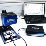
Solar Simulator

Learn More
 Solar Cell Characterizing and Testing
There are several methods used to characterize solar cells. The most common and essential measurement you can take is the current-voltage (I-V) sweep.
Read more... Interpretting J-V Curves
There are many factors which can hinder your device performance including devices shunting, shorting and charge build up.
Read more...References and Further Reading
- Cao, Y. et al., 2018. Direct contact of selective charge extraction layers enables high-efficiency molecular photovoltaics. Joule, Volume 2, pp. 1108-1117.
- Guo, Z. et al., 2021. Dopant-Free Polymer HTM-Based CsPbI2Br Solar Cells with Efficiency Over 17% in Sunlight and 34% in Indoor Light. Advanced Functional Materials, 31(42).
- Jarosz, G., Franz, M., Marczynski, R. & Signerski, R., 2021. Efficiency limit of excitonic photovoltaic cells under phosphor-based white LED illumination. Organic Electronics, 88(105999).
Contributors
Written by
Scientific Writer
Reviewed by
Application Scientist
Diagrams by
Graphic Designer