Tungsten Disulfide (WS2) Monolayer Film
CAS Number 12138-09-9
2D Materials, Low Dimensional Materials, Transition Metal Chalcogenides (TMCs), Transition Metal Dichalcogenides, Tungsten Disulfide
High purity tungsten disulfide monolayer film
For applications in electronic and optoelectronic devices
Technical Data | MSDS | Literature and Reviews
Tungsten disulfide (WS2, CAS number 12138-09-9) monolayer films supersede MoS2 with their superior optical properties, as measured by photoluminescent quantum yield (PLQY) and line-widths. With even larger spin-orbit coupling and nearly three times larger valence band splitting, WS2 monolayer films may exhibit larger band edge spin splittings, stronger valley-Hall effect, and magnetic field effects for optoelectronic and spintronic functionalities.
High Purity
>99% Tungsten Disulfide Purity
Worldwide shipping
Quick and reliable shipping
Low Cost
Low Cost Tungsten Disulfide
Applications
Applications in electronic and optoelectronic devices
Applications
Tungsten disulfide monolayer films show a much higher photoluminescence efficiency and narrower emission line-width than MoS2. Monolayer WS2 films have been widely used in electronic and optoelectronic devices, such as in photovoltaic, FETs, photodetectors, and valleytronic applications.
Synthesis
High-quality tungsten disulfide monolayer films are grown directly on the substrates (sapphire) by the chemical vapour deposition (CVD) method.
Usage
WS2 monolayer films can be used in research purposes such as microscopic analysis, photoluminescence, and Raman spectroscopy studies. Monolayer WS2 films can also be transferred to other substrates.
Technical Data
| CAS Number | 12138-09-9 |
| Chemical Formula | WS2 |
| Molecular Weight | 247.97 g/mol |
| Bandgap | 1.4 - 2.01 eV |
| Synonyms | Tungsten sulphide, Tungsten sulfide, Tungsten(IV) sulfide |
| Classification / Family | Transition metal dichalcogenides (TMDCs), 2D semiconductor materials, Nano-electronics, Nano-photonics, Materials science |
Product Details
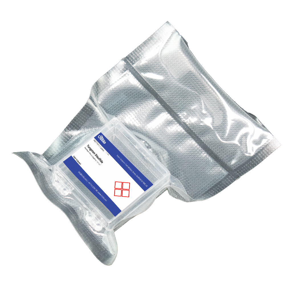
| Substrate | Sapphire |
| Product Code | M2171F11 |
| Size | 1 cm × 1 cm* |
| Growth Method | CVD synthesis |
| Appearance | Transparent |
| Purity | >99% |
| Transparency | >97% |
| Coverage | >95% |
| Number of Layers | 1 |
| Sheet Resistance | N/A |
| Transfer Method | Directly grown |
| Substrate Thickness | 300 µm |
*Other sizes available: up to 2 cm × 2 cm or 2 inches in diameter.
High-quality tungsten disulfide (WS2) monolayer films are available on Sapphire as standard. Different substrates of monolayer WS2 films, including SiO2/Si, Glass, Silicon and Quartz are also available via custom order.
Discontinuous isolated triangular crystals (crystal islands) films are also available via custom request. Please contact us for more information regarding custom products.
Pricing Table
| Product Code | Substrate | Size | Quantity (EA) | Price |
| M2171F11 | Sapphire | 1 cm × 1 cm | 1 | £420 |
MSDS Document
 Tungsten disulfide monolayer film
Literature and Reviews
- Synthesis and Optical Properties of Large-Area Single-Crystalline 2D Semiconductor WS 2 Monolayer from Chemical Vapor Deposition, C. Cong et al., Adv. Optical Mater., 2, 131–136 (2014); DOI: 10.1002/adom.201300428.
- Large-area synthesis of monolayer WS2 and its ambient-sensitive photo-detecting performance, C. Lan et al, Nanoscale, 7, 5974 (2015); DOI: 10.1039/c5nr01205h.
- Electronic properties of WS, monolayer films, A. Klein et al., Thin Solid Films, 380, 221-223 (2000); DIO: 10.1016/S0040-6090(00)01510-8.