Indium(III) Selenide (In2Se3) Powder and Crystal
CAS Number 12056-07-4
2D Materials, Low Dimensional Materials, Materials, Post-Transition Metal Chalcogenides (PTMCs), Transition Metal Chalcogenides (TMCs)
Low price, high purity 2D metal indium(III) selenide powder and crystals
For the development of next-generation electronics, optoelectronics, and nanotechnology
Technical Data | MSDS | Structure | Literature and Reviews | Related Products | Resources and Support
Indium(III) selenide (In2Se3), CAS number 12056-07-4, belongs to the A2IIIB3VI family, and it occurs as several different crystal structures and phases (α, β, γ, δ, and κ). Among those phases, α, β, γ-In2Se3 are semiconducting in nature with layered structures held together via van der Waals. Strong intra-layer chemical valence bonding and weak inter-layer interactions give rise to highly anisotropic structural, electrical, optical, and mechanical properties. This also makes it possible to obtain 2D In2Se3 nanosheets by scaling down to few- or mono-layer.
High Purity
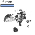
High purity ≥99.999% Indium(III) Selenide(In2Se3) Crystal
Worldwide shipping
Quick and reliable shipping
Low price
Low price Indium(III) Selenide (In2Se3)
Powder & Crystal
Available in Powder & Crystal forms
Among them, α-In2Se3 and β-In2Se3 have been the most-studied phases. However, α-In2Se3 and β-In2Se3 phases share the same rhombohedral crystal structure. Normally, the β-In2Se3 phase only exists at elevated temperatures in bulk single crystals. However, at room temperature it persists in thin layers. This makes it possible for multi-level phase-change memory in a single material system
Few-to-monolayer In2Se3 nanosheets can be obtained through liquid exfoliation of high-purity indium(III) selenide powder - In2Se3. 2D nanosheets and nanoparticles are more compatible with conventional micro-fabrication techniques and they are solution-processable. This makes it easier to build complex structures for advanced electronic and optoelectronic devices
We supply low price indium(III) selenide in powder and crystal forms for a range of applications.
Indium(III) Selenide Powder
Can be used for preparation of indium(III) selenide nanoplates and ultrathin films
Sold by weight
≥99.995% purity
From £220
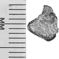
Indium(III) Selenide Crystals by Size
Can be used to produce single or few-layer indium(III) selenide sheets via mechanical or liquid exfoliation
Small (≥10 mm2) or medium (≥25 mm2) crystals available*
≥99.999% purity
From £520
*Typical representative size, areas/dimensions may vary
Bulk single indium(III) selenide crystal is most commonly used as sources from which single or few-layer sheets can be obtained via either mechanical or liquid exfoliation. Single indium(III) selenide crystal or films produced from such crystals are suitable for study using atomic force microscopy or transmission electron microscopy.
Indium(III) selenide powder can also be used to prepare In2Se3 nanosheets and nanoparticles by liquid-exfoliation (normally assisted by sonication), especially when it is the case of foreign elements such as lithium or sodium cations being inserted between layers by the process of intercalation. Liquid exfoliation can provide mass production of such products.
Technical Data
| CAS Number | 12056-07-4 |
| Chemical Formula | In2Se3 |
| Molecular Weight | 466.52 g/mol |
| Bandgap | 1.2 - 3.0 eV |
| Preparation | Synthetic - Chemical Vapour Transport (CVT) |
| Structure | Rhombohedral |
| Electronic Properties | 2D semiconductor |
| Melting Point | 890 °C |
| Colour | Black |
| Synonyms | Indium(III) Selenide, Diindium triselenide |
| Classification / Family | Transition metal dichalcogenides (TMDCs), 2D Semiconductor materials, Charge Density Wave (CDW), Hydrogen Revolution Reactions (HER), Nano-electronics, Nano-photonics, Photovoltaic, Materials science |
Product Details
| Form | Purity |
|---|---|
| Powder | ≥99.995% |
| Crystal | ≥99.999% |
Pricing Table
| Product Code | Form | Size/Weight* | Price |
|---|---|---|---|
| M2136C1 | Powder | 500 mg | £220 |
| M2136C1 | Powder | 1 g | £350 |
| M2136A10 | Crystal | Small (≥10 mm2) | £520 ea. |
| M2136A25 | Crystal | Medium (≥25 mm2) | £850 ea. |
*typical representative size, areas/dimensions may vary
Shipping is free for qualifying orders.
MSDS Documents
 Indium(III) selenide powder
Structure of Indium(III) Selenide
Indium selenide (In2Se3) belongs to the A2IIIB3VI family, and it occurs as several different crystal structures and phases (α, β, γ, δ, and κ). Among those phases, α, β, γ-In2Se3 are semiconducting in nature with layered structures held together via van der Waals. Strong intra-layer chemical valence bonding and weak inter-layer interactions give rise to highly anisotropic structural, electrical, optical, and mechanical properties. This also makes it possible to obtain 2D In2Se3 nanosheets by scaling down to few- or mono-layer.
α-In2Se3 and β-In2Se3 phases share the same rhombohedral crystal structure. The primitive unit cell contains three layers, each consisting of five covalently-bonded, monoatomic sheets in the sequence of Se–In–Se–In–Se. For α-In2Se3, the outer Se-atoms in each layer are aligned, whereas in β-In2Se3 they are located at the interstitial sites of the Se-atoms in the neighbouring layers.

Literature and Reviews
-
Strong quantum confinement effect in the optical properties of ultrathin α-In2Se3, Adv. Opt. Mater., J. Quereda et al., 14 (12), 1939-1943 (2016); DOI: 10.1002/adom.201600365.
- Crystalline–Crystalline Phase Transformation in Two-Dimensional In2Se3 Thin Layers, X. Tao et al., Nano Lett., 13 (8), 3501–3505 (2013); DOI: 10.1021/nl400888p.
- Controlled Synthesis of High-Quality Monolayered α-In2Se3 via Physical Vapor Deposition, J. Zhou et al., Nano Lett., 15 (10), 6400–6405 (2015); DOI: 10.1021/acs.nanolett.5b01590.
Related Products
We stock a wide range of 2D materials available to purchase online. Please contact us if you cannot find what you are looking for.