Graphene Film
CAS Number 1034343-98-0
2D Materials, Graphene Materials, Low Dimensional Materials, Materials
Graphene Film for Applications in Energy Generation and Storage
With a unique combination of novel electronic, optical, and mechanical properties
Overview | Product Information | Related Products
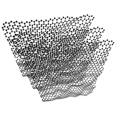
Graphene film (CAS number 1034343-98-0) consists of an atomically-thin layer or multiple ultra-thin layers of carbon atoms that are arranged in a hexagonal honeycomb lattice. When synthesized via chemical vapour deposition (CVD), the structure is polycrystalline in nature, with multiple small graphene domains growing to merge into a continuous film.
Compared to single-layer graphene, few-layer graphene has the potential to be developed into hybrid materials or heterostructures. Different substances can be intercalated into its layered structure.
Our high-quality monolayer graphene films were first grown directly on copper foil via the chemical vapour deposition (CVD) method. The films were later transferred to the desired substrates via the wet chemical graphene-transfer process.
Low Price
Affordable graphene film
High Quality
Monolayer and few-layer films different substrates
Versatile
Ideal for a variety of applications
Worldwide Shipping
Quick and reliable shipping
General Information
| CAS Number | 1034343-98-0 |
|---|---|
| Chemical Formula | CxHy |
| Growth Method | CVD synthesis |
| Form | Film on substrate |
| Appearance | Transparent |
| Purity | >99% |
| Transparency | >97% |
| Coverage | >95% |
| Synonyms | Graphene Graphene Film, Graphene Film |
| Classification or Family | 2D semiconducting materials, Carbon nanomaterials, Nanomaterials, Polycyclic aromatic hydrocarbons, OLEDs, Organic photovoltaics (OPV), Organic electronics |
Graphene Monolayer Film

| Product Code | M2155F11 | M2156F11 | M2315F11 | M2316F11 | M2157F50 |
|---|---|---|---|---|---|
| Number of Layers | 1 | 1 | 1 | 1 | 1 |
| Substrate | SiO2/Si | PET | Sapphire | Quartz | Copper foil |
| Size | 1 cm x 1 cm | 1 cm x 1 cm | 1 cm x 1 cm | 1 cm x 1 cm | 5 cm x 10 cm |
| Transfer Method | Wet chemical transfer | Wet chemical transfer | Wet chemical transfer | Wet chemical transfer | Directly grown |
| Sustrate Thickness | 300 nm (oxide layer) | 250 µm | 300 µm | 1 mm | N/A |
| Sheet Resistance | 400 ± 50 Ohms/sq | 500 ± 50 Ohms/sq | N/A | N/A | 450 ± 40 Ohms/sq |
Graphene Few-Layer Film
| Product Code | M2158F11 | M2159F11 | M2317F11 | M2318F11 | M2160F50 |
|---|---|---|---|---|---|
| Number of Layers | 2 – 6 | 2 – 6 | 2 – 6 | 2 – 6 | 2 – 6 |
| Substrate | SiO2/Si | PET | Sapphire | Quartz | Copper foil |
| Size | 1 cm x 1 cm | 1 cm x 1 cm | 1 cm x 1 cm | 1 cm x 1 cm | 5 cm x 10 cm |
| Transfer Method | Wet chemical transfer | Wet chemical transfer | Wet chemical transfer | Wet chemical transfer | Directly grown |
| Sustrate Thickness | 300 nm (oxide layer) | 250 µm | 300 µm | 1 mm | N/A |
| Sheet Resistance | 400 ± 50 Ohms/sq | 500 ± 50 Ohms/sq | N/A | N/A | 450 ± 40 Ohms/sq |
Custom Graphene Films
Different sizes and substrate types are also available via custom request. Other sizes include 1 cm x 2 cm, 2 cm x 2 cm, or custom-made sizes. Other substrates available are glass, nickel, and silicon.
Please contact us for more details.
MSDS Documentation
Graphene Monolayer
![]() Graphene monolayer film on silicon
Graphene monolayer film on silicon
![]() Graphene monolayer film on PET
Graphene monolayer film on PET
![]() Graphene monolayer film on sapphire
Graphene monolayer film on sapphire
Graphene Few-Layer
![]() Graphene few-layer film on silicon
Graphene few-layer film on silicon
![]() Graphene few-layer film on PET
Graphene few-layer film on PET
![]() Graphene few-layer film on sapphire
Graphene few-layer film on sapphire
Pricing
| Product Code | Substrate | Quantity | Price |
|---|---|---|---|
| M2155F11 / M2158F11 | SiO2/Si | 2 | £250 |
| M2155F11 / M2158F11 | SiO2/Si | 4 | £410 |
| M2156F11 / M2159F11 | PET | 2 | £250 |
| M2156F11 / M2159F11 | PET | 4 | £410 |
| M2315F11 / M2317F11 | Sapphire | 2 | £250 |
| M2315F11 / M2317F11 | Sapphire | 4 | £410 |
| M2316F11 / M2318F11 | Quartz | 2 | £250 |
| M2316F11 / M2318F11 | Quartz | 4 | £410 |
| M2157F50 / M2160F50 | Copper foil | 1 | £520 |
More on Graphene Film
Graphene film was first isolated via mechanical exfoliation, also known as the Scotch-tape method. Chemical vapour deposition (CVD) and epitaxial methods were later developed and commonly used as alternative methods for growing research-grade single, bilayer, and few-layer graphene films. Graphene films can also be transferred to other substrates.
References
- Transfer of CVD-Grown Monolayer Graphene onto Arbitrary Substrates, J. Suk et al., ACS Nano, 5 (9), 6916–6924 (2011); DOI: 10.1021/nn201207c.
- Raman Studies of Monolayer Graphene: The Substrate Effect, Y. Wang et al., J. Phys. Chem. C, 112 (29), 10637–10640 (2008); DOI: 10.1021/jp8008404.
- Large-scale pattern growth of graphene films for stretchable transparent electrodes, K. Kim et al., Nature, 457, 706–710 (2009); doi: 10.1038/nature07719.
Related Products
We stock a wide range of 2D materials available to purchase online. Please contact us if you cannot find what you are looking for.