Hafnium Diselenide (HfSe2) Powder and Crystal
CAS Number 12162-21-9
2D Materials, Low Dimensional Materials, Transition Metal Chalcogenides (TMCs), Transition Metal Dichalcogenides
Please choose the appropriate MSDS from the list below. Links will open in a new window. If your browser does not support PDFs, you will be prompted to download the file instead.
Low price, high purity 2D hafnium diselenide powder and crystals
For the development of next-generation electronics, optoelectronics, and nanotechnology
Technical Data | MSDS | Structure | Literature and Reviews
Hafnium diselenide (HfSe2), CAS number 12162-21-9, is a layered 2D semiconducting material. It is part of the group IV transition metal dichalcogenides (TMDCs).
2D semiconductor HfSe2 is increasing in popularity for use in electronic devices due to the existence of natively-compatible HfO2 with desirable high-κ dielectrics. It is one of the first 2D materials to emulate the technologically-relevant properties of silicon (whilst enabling lower operation power than possible with silicon and its silicon oxide insulator) on a atomically-thin and smaller circuit.
High Purity
High purity 2D hafnium diselenide
Worldwide shipping
Quick and reliable shipping
Low price
Low price Hafnium Diselenide
Powder & Crystals
Available in powder and crystal forms
HfSe2 has an indirect bandgap with a measured bulk value of Eg = 1.1 eV (similar to that of silicon) and a remarkably high phonon-limited mobility of about 3500 cm2/V·s at room temperature.
We supply low price hafnium diselenide in several different forms for a range of applications.

Hafnium Diselenide Powder
Can be used for preparation of hafnium diselenide nanoplates and ultrathin films
Available in quantities of 1 g
≥99.995% purity
From £350

Hafnium Diselenide Crystals by Size
Can be used to produce single or few-layer hafnium diselenide sheets via mechanical or liquid exfoliation
Small (≥10 mm2) or medium (≥25 mm2) crystals available*
≥99.999% purity
From £520
*Typical representative size, areas/dimensions may vary.
Bulk single hafnium diselenide crystal is most commonly used as sources from which single or few-layer sheets can be obtained via either mechanical or liquid exfoliation. Single hafnium diselenide crystal or films produced from such crystals are suitable for study using atomic force microscopy or transmission electron microscopy.
Few-layer HfSe2 nanosheets and nanoparticles can also obtained from hafnium diselenide powder by liquid-exfoliation.
Technical Data
| CAS Number | 12162-21-9 |
| Chemical Formula | HfSe2 |
| Molecular Weight | 336.43 g/mol |
| Bandgap | ~1.1 eV (indirect) |
| Preparation | Synthetic - Chemical Vapour Transport (CVT) |
| Structure | Octahedral (1T) |
| Electronic Properties | 2D Semiconductor |
| Melting Point | N/A |
| Colour | Dark brown |
| Synonyms | Hafnium selenide, Bis(selanylidene)hafnium |
| Classification / Family | Transition metal dichalcogenides (TMDCs), 2D Semiconductor materials, Nano-electronics, Nano-photonics, Photovoltaic, Materials science |
Product Details
| Form | Purity |
| Powder | ≥99.995% |
| Crystal | ≥99.999% |
Pricing Table
| Product Code | Form | Size/Weight* | Price |
| M2153C1 | Powder | 1 g | £350 |
| M2153A10 | Crystal | Small (≥10 mm2) | £520 ea. |
| M2153A25 | Crystal | Medium (≥25 mm2) | £850 ea. |
*typical representative size, areas/dimensions may vary.
Shipping is free for qualifying orders.
Key Product Data
- High purity hafnium diselenide suitable for a range of applications
- Available in powdered form or in crystal form by weight or size
- Low price with free worldwide shipping on qualifying orders
MSDS Documents
Structure of Hafnium Diselenide
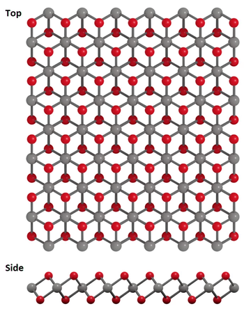
HfSe2 adopts the CdI2 structure (1T), consisting of a single-layer plane of hexagonal close-packed Hf atoms sandwiched by two-layer planes of hexagonal close-packed Se atoms. The Hf atom is octahedrally coordinated with six selenide chalcogen atoms. The layers are stacked together by weak van der Waals (vdW) forces, and can be exfoliated into thin 2D layers.

Properties of Hafnium Diselenide
After exfoliation of hafnium diselenide crystal or powder, hafnium diselenide typically has the following properties:
- Octahedral (1T, space group: P3m1)
- Group IV transition metal dichalcogenides (TMDCs)
- HfSe2 has an indirect bandgap with a measured bulk value of Eg = 1.1 eV (similar to that of silicon)
- Remarkably high phonon-limited mobility of about 3500 cm2/V·s at room temperature
- One of the first 2D materials to emulate the technologically-relevant properties of silicon
Applications of Hafnium Diselenide
Hafnium diselenide (HfSe2) single crystals can be used to prepare monolayer and few-layer HfS2 by mechanical or liquid exfoliation.
Hafnium diselenide powder is suitable for liquid chemical exfoliation to prepare HfSe2 nanosheets and nanoparticles down to few-layer films.
Hafnium diselenide is slightly n-type with an indirect band gap of ∼1.1 eV, making it a great candidate for field-effect transistors and photovoltaic applications. Au-contacted HfSe2 phototransistors give a high on/off ratio of 106 and mobilities in the range of 2.6–6.5 cm2 V−1 s−1, with a high responsivity of 252 A/W and an ultrafast response time of 7.8 ms.
Hf-based TMDs are small bandgap semiconductors possessing large work functions and reasonably high mobility. They are suitable for photovoltaic and FET applications. Ultrathin nanosheets of HfSe2 can also be built into ultrafast and ultrasensitive phototransistor devices.
Literature and Reviews
- Two-dimensional semiconductor HfSe2 and MoSe2/HfSe2 van der Waals heterostructures by molecular beam epitaxy, K. E. Aretouli et al., Appl. Phys. Lett. 106, 143105 (2015); doi: 10.1063/1.4917422.
- Tunable electrical properties of multilayer HfSe2 field effect transistors by oxygen plasma treatment, M. Kang et al., Nanoscale, 9, 1645 (2017); DOI: 10.1039/c6nr08467b.
- 3d transition metal doping-induced electronic structures and magnetism in 1T-HfSe2 monolayers, X. Zhao et al., RSC Adv., 7, 52747–52754 (2017); DOI: 10.1039/c7ra11040e.
Related Products
We stock a wide range of 2D materials available to purchase online. Please contact us if you cannot find what you are looking for.

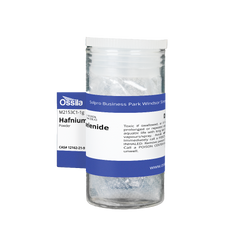
 Hafnium diselenide powder

