How To Read An Absorbance Spectrum

Molecule Identification | Conjugated Organics | Measuring Material Properties of Semiconductors | Solution Concentration and Optical Density
Material Purity | Identify Aggregates and Complexes | Characterizing Device Layers | Other Uses
There are many material properties and phenomena that can be measured with absorbance spectroscopy. The key to unlocking these insights lies in carefully reading absorbance spectra and interpreting spectral properties they reveal.
UV-Vis absorbance spectroscopy is a versatile, low cost technique that can characterize materials with allowed energy transitions between 1-4 eV. It can be performed using a range of equipment, from can be done by a range of different spectroscopy equipment, from a dedicated spectrofluorometer to modular USB spectrometers. This technique can be used to study chemical dyes, chromophores, conjugated organic materials, or materials whose properties of interest are in the visible region, such as solar cells or OLEDs. You can also use optical spectroscopy to measure the concentration of that specific material.
The most important features to identify in most spectra are any absorbance peaks, intensity changes and peak shifts. In more absorbent samples, other interesting features include absorbance edges. Using these features, you can gain information about a range of materials by simply looking at their absorbance spectrum.
Absorbance Measurement Equipment


Molecule Identification
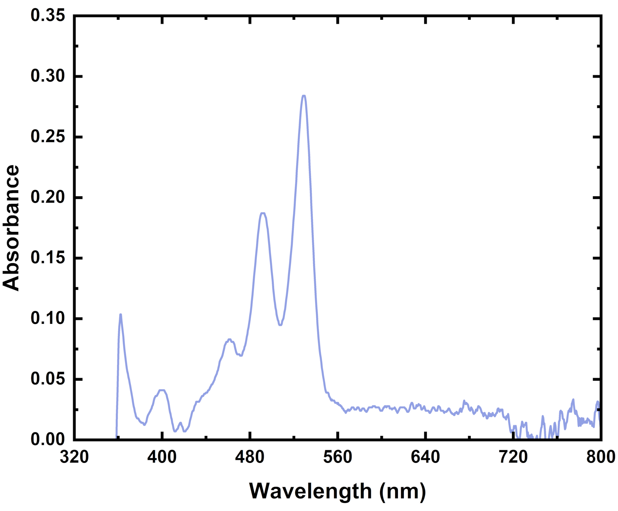
Practically everything has a recorded absorbance spectrum. Therefore, you can use an absorbance spectrum of your material to identify different molecular structures within a solution or film. You can also use it to help determine the ratios of various molecules within a solution or a film.

In the above example, you can see peaks that align with P3HT. You can also see some peaks that align with o-IDTBR in the mixed polymer blend. The location and intensity of these peaks can help you work out how much of each material is in a film and how these materials have interacted with one another.
Conjugated Organics
Conjugated organic molecules are molecules with alternating single and double carbon bonds. This means they have conjugated pi-bonds associated with them, and therefore have additional pi and anti-pi energy levels. Only certain electronic transitions can be detected using optical spectroscopy (π → π, Σ → π) and these different energy transitions will lead to different absorbance peaks.
Optical spectroscopy is incredibly useful if you want to determine the amount of pi-conjugation within a molecule. An increase in the amount of conjugation in a molecule will cause a bathochromic shift. You can measure the levels of aggregation of pi-conjugation in a solution or a material non-invasively using an optical spectrometer.
Measuring Material Properties of Semiconductors
You can determine a semiconductors band gap using absorbance spectroscopy via the Tauc equation.

Where A is an optical constant, h is Planck's constant, α is absorption coefficient, Eg is the material's band gap, and v is the frequency of the photon. γ is a factor that varies depending on the nature of the electronic transition. For direct bandgap transitions, it is equal to 0.5. For indirect bandgap transitions, it is equal to 2.
For direct band gap semiconductors, you can find the band gap of a material using optical absorption by plotting (αhν)2 against hv. By applying a linear fit to the absorbance edge of this plot, the x-intercept will give you the material band gap.
For several composite semiconductors, band gap changes can indicate changes in material composition. For example, in perovskite solar cells, incorporation of bromine into the crystal lattice will shift the band gap to a lower wavelength. This will indicate an increase in the band gap.
Determining Solution Concentration and Optical Density
The concentration of a molecule in a solution or film can be determined using Beer-Lambert's law. One experimental way to measure the concentration of a molecule in a sample is to create a graph of absorbance vs. concentration for that material. To do this, you will need to measure the absorbance coefficient at a chosen wavelength for a range of known concentrations. You should choose the wavelength where there is a significant absorbance peak in your spectrum. However, if you have other materials in your sample, ensure this peak doesn't overlap with any other material peaks. As an example, we have done this using the organic dye BOPIDY below.

Here, we will be measuring the absorbance variation at 533 nm, where there is a large absorbance peak. By plotting the absorption coefficient against concentration, we can create a standard graph. We can then use this to determine the direction of molar concentration from the absorbance coefficient.

You can also use optical spectroscopy to track the growth of bacteria in a cell culture. If you use a clear medium, as the amount of bacteria increases, the absorbance of your culture will increase massively. By plotting a bacterial growth curve, you can follow these stages of bacterial growth. This is especially useful if you are working on any antimicrobial technology.
Identifying Purity of Materials
Absorbance spectroscopy can be an easy way to check the purity of any material if it has absorbance peaks within the region of your USB spectrometer. To do this, take an absorbance spectrum of your materials, either in solution or spin coated into a film. By comparing the absorbance peaks with a reference spectrum, you will be able to pick out any peaks from material impurities.
Optical absorbance is often used for this in industrial applications, acting as a quick and easy way to check the quality of metal alloys. It can also be used for biological applications, where risks of contamination can threaten sterile environments.
Identifying Aggregates and Complexes
At a low enough concentration, using UV-Vis spectroscopy can help you explore the formation of complexes in solution or even aggregates in films. Measuring the amount of coordination in solutions will inform you about whether the material you are measuring is interactive. It can also provide information about how other molecules are interacting within the sample you are measuring.
Examples where complexes and coordination are studied using UV-Vis spectroscopy include:
- At low wavelengths, the types of Pb-halide co-ordination can be determined using UV-Vis spectroscopy. This can be very informative when you want to recognize the influence of other materials (solvents/organic cations) on crystal structure.
- The formation of H/J aggregates in polymer morphology can be detected using optical spectroscopy. If H aggregates are forming, you will see blue shift in your absorption spectra towards lower wavelengths compared to the monomer. However, J aggregation will lead to the formation of a sharp peak that is redshifted compared to the monomer peak.
- In determining how nickel(II) and cobalt(II) benzhydrazone complexes interact with DNA protein receptors. This can also be detected at low wavelengths (<400 nm) using UV-Vis spectroscopy.
Characterizing Device Layers
Most optical or optoelectronic devices require multiple layers in order to work effectively.
The optical properties of these layers will depend entirely on their function. You will need to characterize this, as well as the entire device, independently. Additionally, supplementary layers can be introduced into a device to improve its optical properties.
Examples of these layers and their desired optical characterization include:
- Antireflective layers which can be placed on top of devices that absorb light, with the aim of increasing the amount of light that can be absorbed. This should result in an increase in the absorbance peaks.
- Charge transport layers that surround a device shouldn't be parasitically absorbing light. Absorbance measurements can ensure that these layers do not absorb in the same region as the absorbing molecules.
- Light shifting molecules which can be placed in the path of light entering or leaving a device to get rid of unwanted light. For example, luminescent, down-shifting layers can absorb UV-light and convert it into visible light. This will increase the amount of usable light that reaches a solar cell.
Other Uses for Absorbance Spectroscopy
Other useful ways which you can use absorbance spectroscopy:
- To determine the glass transition temperature of polymer films.
- To track reactions in your solution using universal indicators.
- To test electrochromic materials (which change color depending on the electrical stimulus).
- To measuring the size of certain nanoparticles.
Spectroscopy Equipment & Components

Learn More
 Absorbance Measurement
Absorbance measurements are crucial in many areas of scientific research. This article describes how to take an absorbance measurement using an optical spectrometer.
Read more... Absorbance Measurements with the Ossila Spectrofluorometer
Absorbance spectroscopy is capable of revealing critical information about a sample's molecular structure, concentration, and optoelectronic behaviour, and can even track dynamic changes such as shifts in phase or chemical composition. This guide demonstrates how to use the Ossila Spectrophotometer or Spectrofluorometer to take reliable absorbance measurements.
Read more...References
- Rocha, F. S., Gomes, A. J., Lunardi, C. N., Kaliaguine, S., & Patience, G. S. (2018). Experimental methods in chemical engineering: Ultraviolet visible spectroscopy-UV-vis. The Canadian Journal of Chemical Engineering, 96(12), 2512–2517. DOI:10.1002/cjce.23344
- Hestand, N. J., & Spano, F. C. (2018). Expanded theory of H- and J-molecular aggregates: The effects of vibronic coupling and intermolecular charge transfer. Chemical Reviews, 118(15), 7069–7163. DOI: 10.1021/acs.chemrev.7b00581
- Makuła, P., Pacia, M., & Macyk, W. (2018). How to correctly determine the band gap energy of modified semiconductor photocatalysts based on UV–vis spectra. The Journal of Physical Chemistry Letters, 9(23), 6814–6817. DOI: 10.1021/acs.jpclett.8b02892
- Chen, J., Zhou, S., Jin, S., Li, H., & Zhai, T. (2016). Crystal organometal halide perovskites with promising optoelectronic applications. Journal of Materials Chemistry C, 4(1), 11–27. DOI: 10.1039/c5tc03417e