Viscoelastic Transfer of 2D Material Using PDMS
Viscoelastic transfer using polydimethylsiloxane (PDMS) stamps is one of the methods used for the deterministic placement of 2D materials and the fabrication of van der Waals heterostructures [1]. It relies on the viscoelasticity of PDMS, which behaves as an elastic solid on short time scales, but as a viscous fluid on long time scales. As a result, PDMS films demonstrate kinetically controlled adhesion: the faster an object is pulled off the surface of the film, the stronger adhesion force it will experience. Faster peel-off rates therefore can be used to deposit 2D material onto PDMS, and slower rates - to release it onto a target substrate.
PDMS-based transfer offers a fast and convenient way of depositing 2D materials onto virtually any substrate and, unlike other methods, does not require the use of wet chemistry. One significant limitation of this technique are polymer residues left on the surface of the material after the transfer. These residues are generally inert and optically clear, and their presence might be beneficial for the optical properties of 2D crystals, acting as an encapsulation layer that protects the material from the surrounding environment. They can, however, prevent efficient interaction between different layers, and van der Waals heterostructures fabricated using this method usually require additional processing steps, such as thermal annealing or AFM ironing [2] to improve the quality of the interlayer interface. This technique is therefore best suited for the fabrication of individual monolayers and their integration into existing structures, such as pre-pattern contacts, photonic and plasmonic structures.
UV Ozone Cleaner

- Ultraclean Surfaces within Minutes
- Worldwide Shipping
Buy Online £2500
Video Guide (Part 1) - Exfoliation and Flake Identification
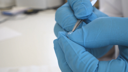
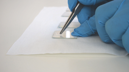
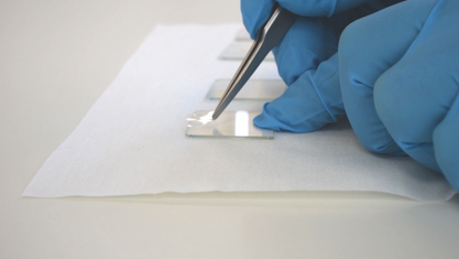
Preparation of the PDMS Stamp
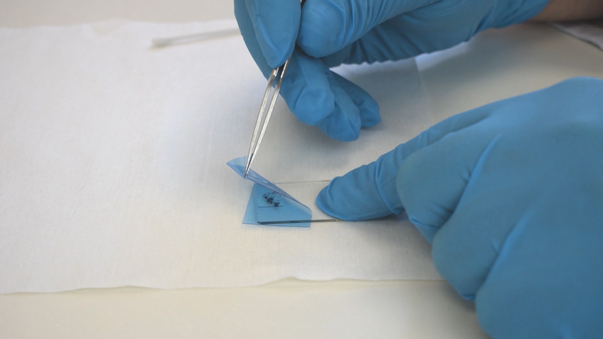
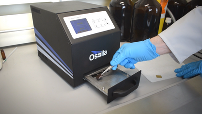
PDMS is a commercially available rubber, commonly used as protective coating for solar cells and light-emitting diodes. In this guide, we will be using pre-packaged films available from Gel-Pak (product code PF-3-X4), but two-component elastomer kits (such as Sylgard 184 from Dow Corning) can also be used. For viscoelastic transfer, a thin PDMS film (<1 mm) is deposited onto a rigid transparent substrate, such as microscope glass slide, which acts as a support for mechanical exfoliation and transfer.
2D Materials
- High-Quality Materials
- Low Price
- Worldwide Shipping
Available From £105
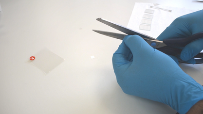
Exfoliation
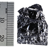
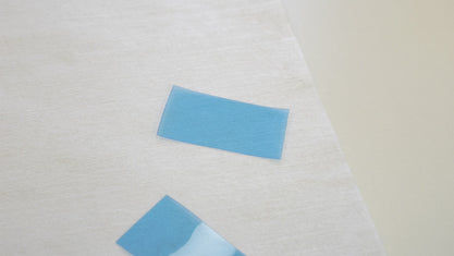
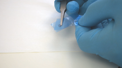
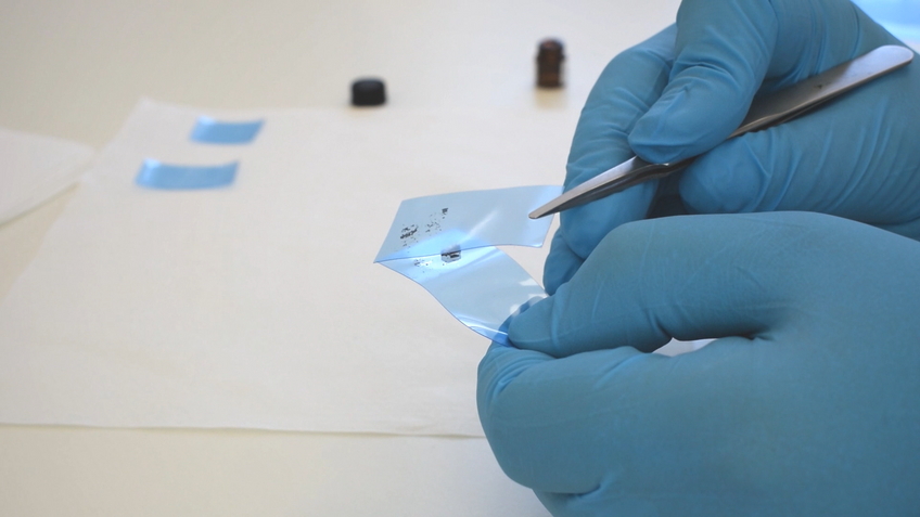
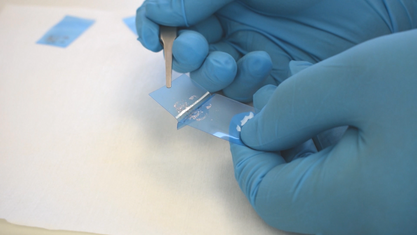
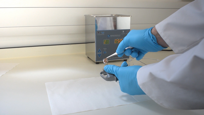
Mechanical exfoliation is the method originally developed by Andre Geim and Konstantin Novoselov for the isolation of monolayer graphene in 2004 and has been successfully applied to other layered materials. Despite low yield and relatively small size of the single-layer flakes produced by this technique, it is still widely used in research due to its accessibility and excellent material quality of the produced samples. Single, and few-layer flakes are separated from bulk crystal and deposited onto a substrate using a piece of adhesive tape. We use high-quality tape (BT-150E-CM, Nitto) designed to minimise tape residues, but normal office tape, such as Magic Tape from Scotch, could also be used.
Flake Search and Thickness Identification
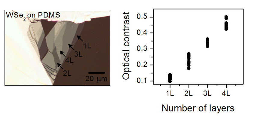
Mechanical exfoliation produces flakes of various sizes and thicknesses; atomically thin flakes are a minority among much thicker crystals. These flakes need to be located and identified using a reflected-light microscope - a process commonly known as flake search. Mono, and few-layer flakes can be distinguished by their translucent appearance and low optical contrast. Their visibility will depend on the material, substrate it is deposited on, and the optical system used. Materials with higher absorption in visible range, such as transition metal dichalcogenides, will be more visible than materials with weaker absorption such as graphene or hexagonal boron nitride. Certain types of substrates, such as silicon wafers covered with a 90 nm or 290 nm thick silicon dioxide layer, can improve the flake visibility. Once a suspected monolayer flake is located, its thickness can be estimated using optical contrast measurements and confirmed using Raman or photoluminescence spectroscopy.
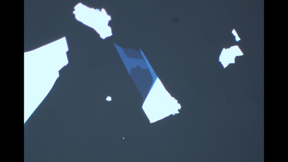
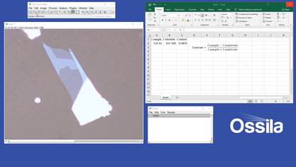
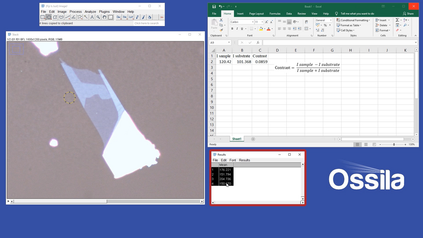

The optical contrast of layered 2D materials changes linearly with increasing number of layers. The value of the contrast can be positive or negative, depending on the type of the substrate used, and might also vary depending on the measurement conditions. However it should be close to the minimum difference between the adjacent thicknesses.

Video Guide (Part 2) - Deterministic Transfer
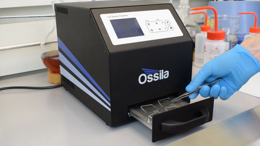
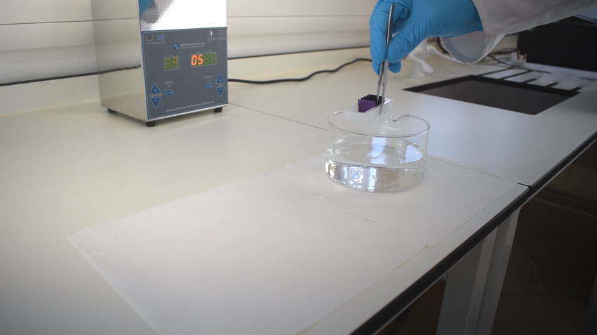
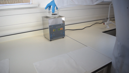
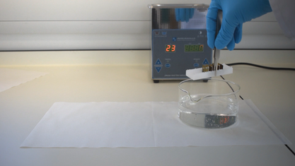
Target Substrate Cleaning
The cleanliness of the target substrate plays a key role in the deterministic transfer process, affecting both the success of the transfer and the quality of the resulting sample. The cleaning method will depend on the type of substrate used – here we will discuss the cleaning of a silicon substrate coated with 300 nm thick thermally grown SiO2 layer, the type of substrate commonly used in 2D material research.
UV Ozone Cleaner
- Ultraclean Surfaces within Minutes
- Worldwide Shipping
Buy Online £2500
Initial Alignment
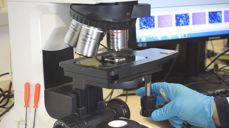
Deterministic transfer of 2D materials requires a dedicated transfer setup, which comprises two key components: a set of micromanipulators for precise alignment of the polymer film with the transferred material and the target substrate, and a long working distance reflected light microscope equipped with a digital camera. Depending on the transfer method used, the setup might also include a heated holder for the target substrate. A bare minimum requirement for PDMS transfer is a 3-axis micromanipulator for the stamp alignment, and a digital camera with a zoom lens.
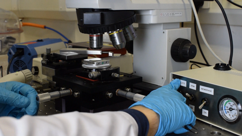
1. If your transfer system allows pitch and roll adjustments, use them to ensure that the glass slide with the PDMS stamp is parallel to the target substrate. A small degree of pitch misalignment might be beneficial for the transfer, as it will allow the stamp to come into contact with the substrate and detach from it in a more gradual way.
2. Put the target substrate onto the substrate holder and fix it in place with double sided adhesive tape or vacuum. Using the X and Y translation stages, place the target area of the substrate in the centre of the field of view. A PDMS transfer will be easier to achieve if you choose a region at the edge of the substrate on the side closest to the stamp holder, as this will minimise the area of contact between the stamp and the substrate surface.
3. Focus the microscope on the substrate and inspect it to make sure the chosen target region is free of contamination. Having a feature on the substrate, such as a scratch mark or a small dust particle in the vicinity of the target region will make it easier to identify the optimal focus point (especially if you are transferring a 2D flake onto a bare substrate). If you are struggling to find the optimal focus, close the field diaphragm of the microscope until its leaves are visible and adjust the focus again – the leaves should come into sharp focus at the same time as the substrate surface.
4. Attach the glass slide (PDMS stamp facing down) to the 3-axis micromanipulator. Close the aperture diaphragm of the microscope all the way to improve the contrast of the image. Then focus the microscope on the stamp surface and locate the transferred flake, placing it roughly in the centre of the field of view.
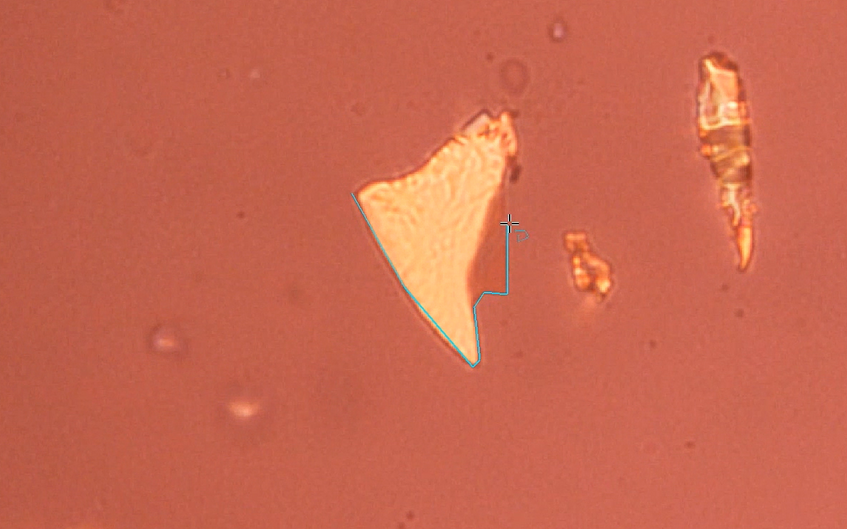
5. Draw the outline of the flake in the microscope software. If necessary, mark any flakes in its vicinity that might interfere with the transfer. If the software that you use does not support marking, you can use software such as Peek Through to overlay a semi-transparent image of the flake outline on top of the microscope software window.
6. Bring the focus down until the substrate looks sharp. Using the outline of the flake that you drew, adjust the position of the substrate to align the flake to the target area. Make sure that other flakes surrounding it do not overlap with important features on the substrate (e.g. bridge a contact pair).
Deterministic Transfer
Once the initial alignment is complete, you can proceed to the final step of the transfer process which consists of bringing the stamp in contact with the substrate while maintaining the required alignment. Then slowly separate the two, leaving the 2D crystal on the target substrate. The peel off rate plays a crucial role in the success of the transfer – using a manual differential micrometer screw or a motorised actuator for Z axis will give you much finer control.
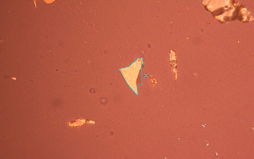
1. Bring the stamp closer to the substrate surface while maintaining sufficient vertical separation. The best way to do this is to focus on the substrate surface, then bring the focus up by ~100 μm and lower the glass slide until the surface of the stamp comes into sharp focus. Use the markings on the fine focus knob to identify the required number of rotations – for modern Nikon microscopes, 100 μm usually corresponds to one full rotation.
2. Check the alignment of the transferred flake. If the PDMS stamp has shifted, adjust its position until the flake is aligned with the outline that you drew.
3. Continue to lower the stamp while observing the flake alignment, until you get close to the substrate surface.
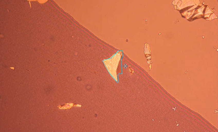
4. Focus on the substrate and keep lowering the glass slide until a part of the stamp comes in contact with the substrate. The point of contact can be identified by a change of colour and contrast.
5. Continue to bring the stamp down until the area of the stamp (~100 μm radius around the flake) is in contact with the substrate. Increasing the area of contact further will result in more pressure being applied to the flake. This can ensure better contact with the substrate but may also lead to formation of cracks and wrinkles.
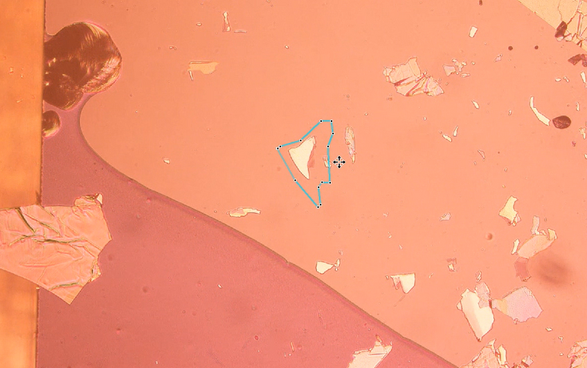
6. Start to slowly lift the stamp up. As the adhesion of the PDMS stamp is kinetically controlled, the slower you separate the stamp from the substrate, the more likely the flake will be transferred. Peel off rate can be kept reasonably high at a large distance (>50 μm) from the flake, but should be as slow as possible in its close vicinity.
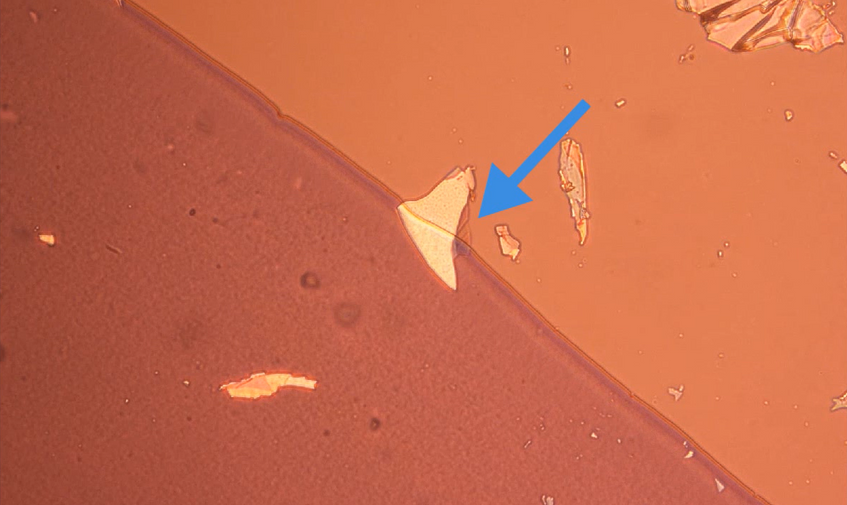
7. When the contact line approaches the flake, switch to a higher-magnification lens and look for a subtle change in colour in the thin regions. This indicates that it is being successfully transferred.
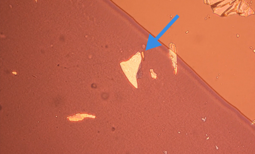
8. A lack of contrast variation and movement of the flake shows that it is being lifted with the stamp – you can try to lower the stamp and make another transfer attempt.
9. Once the contact line is at a sufficient distance from the flake (>100 μm), you can increase the rate of peel off. However, trying to lift the stamp too quickly might make the adhesion too strong, resulting in the whole substrate being lifted by the stamp.
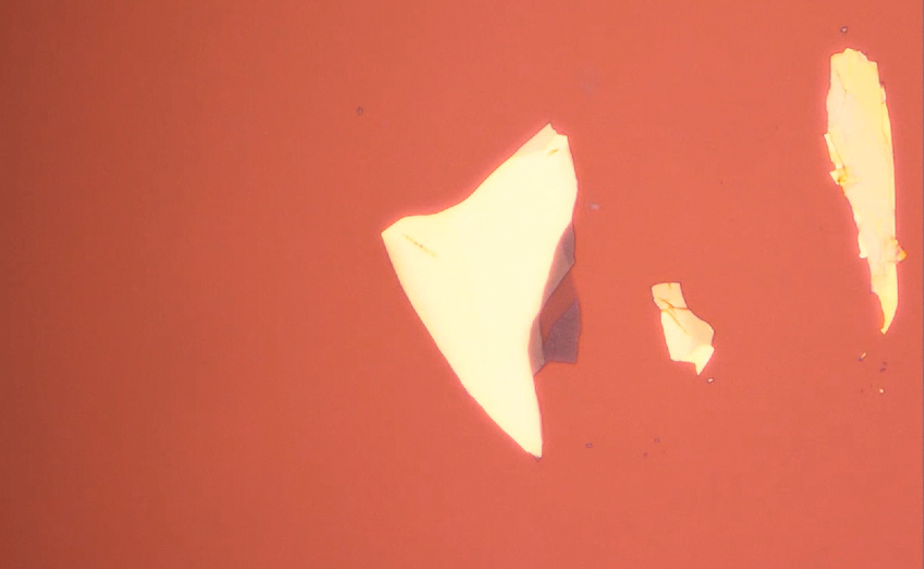
10. Lift the stamp up until it is fully separated from the substrate, then remove the glass slide and inspect the transferred flake. Don’t forget to open the aperture diaphragm of the microscope.
Further Reading
- Novoselov, K. S., Mishchenko, A., Carvalho, A. & Castro Neto, A. H. 2D materials and van der Waals heterostructures. Science (80-. ). 353, aac9439 (2016) – a comprehensive review of 2D materials and van der Waals heterostructures.
- Huang, Y. et al. Reliable Exfoliation of Large-Area High-Quality Flakes of Graphene and Other Two-Dimensional Materials. ACS Nano 9, 10612–10620 (2015) – a paper detailing mechanical exfoliation of 2D materials onto SiO2 /Si substrate.
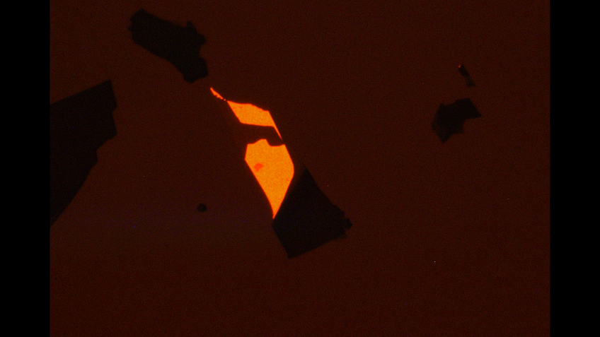
- Alexeev, E. M. et al. Imaging of Interlayer Coupling in van der Waals Heterostructures Using a Bright-Field Optical Microscope. Nano Lett. 17, 5342–5349 (2017) – a paper from our group showing how a bright-field microscope can be used for photoluminescence imaging of monolayer TMDs and their heterostructures.
- Jain, A. et al. Minimizing residues and strain in 2D materials transferred from PDMS. Nanotechnology 29, 265203 (2018) and Schwartz, J. J. et al. Chemical Identification of Interlayer Contaminants within van der Waals Heterostructures. ACS Appl. Mater. Interfaces acsami.9b06594 (2019). doi:10.1021/acsami.9b06594 – two papers describing methods of reducing surface contamination in PDMS-transferred samples.
- Castellanos-Gomez, A. et al. Deterministic transfer of two-dimensional materials by all-dry viscoelastic stamping. 2D Mater. 1, 011002 (2014).
- Frisenda, R. et al. Recent progress in the assembly of nanodevices and van der Waals heterostructures by deterministic placement of 2D materials. Chem. Soc. Rev. (2017). doi:10.1039/C7CS00556C
References
- Castellanos-Gomez, A et al. 2014, ‘Deterministic transfer of two-dimensional materials by all-dry viscoelastic stamping’, 2D Materials, vol. 1, no. 1.
- Rosenberger, M et al. 2018, ‘Nano-“Squeegee” for the Creation of Clean 2D Material Interfaces’, ACS Applied Materials & Interfaces, vol. 10, no. 12. pp. 10379-10387
- Ferrari, A. C. et al. 2006, ‘Raman Spectrum of Graphene and Graphene Layers’, Physical review letters, vol. 97, no. 18.
- Gorbachev, R. V. et al. 2011, ‘Hunting for Monolayer Boron Nitride: Optical and Raman Signatures’, Small, vol. 7, no. 4, pp 465-468.
- Tonndorf, P. et al. 2013, ‘Photoluminescence emission and Raman response of monolayer MoS2, MoSe2, and WSe2’, Optics Express, vol. 21, no. 4, pp. 4908-4916.