Hexagonal Boron Nitride (h-BN) Crystals and Films
CAS Number 10043-11-5
2D Materials, Hexagonal Boron Nitride, Low Dimensional Materials
Please choose the appropriate MSDS from the list below. Links will open in a new window. If your browser does not support PDFs, you will be prompted to download the file instead.
Low price, high purity 2D hexagonal boron nitride (h-BN) crystals and films
Suitable for the creation of single or few-layer sheets via mechanical or liquid exfoliation
Technical Data | MSDS | Structure | Literature and Reviews
With a honeycomb structure based on sp2 covalent bonds similar to graphene, hexagonal boron nitride (CAS number 10043-11-5) is also known as “white graphene”. h-BN monolayers have a layered structure (again, very similar to graphene).
The hexagonal crystal structure of h-BN is one of the three crystalline forms of boron nitride (BN). BN crystallises in hexagonal form at room temperature and normal pressure. It is the most stable phase of the three crystalline forms. At higher temperature and pressure, h-BN transform into a wurtzite structure (P63mc).
High Purity
High purity ≥99.99% Hexagonal Boron Nitride Cystal
Worldwide shipping
Quick and reliable shipping
Low price
Low price Hexagonal Boron Nitride (h-BN)
Film & Crystals
Available in Film and crystal forms
h-BN is normally considered an insulator, and is used as a sub-layer material for any other 2D material in electronic devices. However, it has exotic opto-electronic properties (e.g. wide bandgap and low dielectric constant) along with mechanical robustness, high thermal conductivity and chemical inertness. It was later confirmed to have an indirect bandgap (at 5.955 eV), and thus is also considered a semiconductor.
2D h-BN has no absorption in the visible range, but has absorption in the ultraviolet region with good photoluminescence.
Hexagonal boron nitride (h-BN) monolayer film has a similar lattice structure to graphene, with a lattice mismatch of only about 1.8%. h-BN and graphene are different in terms of their electrical conductivity. With a bandgap of 6.08 eV, h-BN has an insulating nature, whereas graphene is considered a semi-metal.
h-BN is widely used as a dielectric substrate in electronic and optical devices for graphene and other 2D-layered semiconductors (e.g. transition metal dichalcogenides TMDs).
Hexagonal boron nitride (h-BN) few-layer film, often referred to as h-BN nanosheets (h-BNNS), has an ultra-flat surface without dangling bonds. Due to its oxidation resistance even at high temperatures (up to 1000 oC) and chemical resistance to both acids and bases, it is believed to be a better substrate than silicon.
We supply low price hexagonal boron nitride (h-BN) in several different forms for a range of applications.

Hexagonal Boron Nitride Crystals
Can be used for preparation of hexagonal boron nitride nanoplates and ultrathin films
Available in Pack of 5 or 10 crystals
≥99.99% purity
From £520

Hexagonal Boron Nitride by Size
Can be used as substrate, dielectrics and passivation laayers or interlayer to other 2D materials
Monolayer and few-layer h-BN films available on SiO2/Si or PET substrate*
≥99.99% purity
From £250
*Custom made size and substrates are also available
- Glass (1 cm × 1 cm, 1 cm × 2 cm, 2 cm × 2 cm or custom-made sizes)
- Sapphire (1 cm × 2 cm, 2 cm × 2 cm or custom-made sizes)
- Silicon (1 cm × 2 cm, 2 cm × 2 cm or custom-made sizes)
- Quartz (1 cm × 2 cm, 2 cm × 2 cm or custom-made sizes)
- Copper (5 cm × 10 cm or custom-made sizes)
Hexagonal boron nitride (h-BN) crystals are most commonly used as sources from which single or few-layer sheets can be obtained via either mechanical or liquid exfoliation.
h-BN has been used as a protective membrane in devices such as deep ultraviolet and quantum photonic emitters, where it provides strong oxidation resistance. It has also been utilised as a tunnelling barrier in field-effect tunnelling transistors.
Technical Data
| CAS Number | 10043-11-5 |
| Full Name | Hexagonal boron nitride |
| Chemical Formula | BN |
| Molecular Weight | 24.82 g/mol |
| Bandgap | Indirect bandgap at 5.955 eV |
| Preparation | Synthetic - Chemical Vapour Transport (CVT) |
| Structure | Hexagonal (2H) |
| Electronic Properties | 2D Materials - insulator/semiconductor |
| Melting Point | 2,973 °C (sublimates) |
| Colour | Colourless |
| Synonyms | White graphene, hexagonal BN, h-BN |
| Classification / Family | 2D materials, Organic electronics, Materials science |
Product Details
| Form | Purity |
| Crystal | ≥99.99% |
| Film | ≥99% |
Monolayer Film
| Substrate | SiO2/Si | PET | Sapphire | Quartz |
| Product Code | M2161F11 | M2162F11 | M2319F11 | M2320F11 |
| Size | 1 cm × 1 cm* | 1 cm × 1 cm* | 1 cm × 1 cm* | 1 cm × 1 cm* |
| Growth Method | CVD synthesis | CVD synthesis | CVD synthesis | CVD synthesis |
| Appearance | Transparent | Transparent | Transparent | Transparent |
| Purity | >99% | >99% | >99% | >99% |
| Transparency | >97% | >97% | >97% | >97% |
| Coverage | >95% | >95% | >95% | >95% |
| Number of Layers | 1 | 1 | 1 | 1 |
| Sheet Resistance | n.a. | n.a. | n.a. | n.a. |
| Transfer method | Wet chemical transfer | Wet chemical transfer | Wet chemical transfer | Wet chemical transfer |
| Substrate Thickness | 300 m (oxide layer) | 250 µm | 300 µm | 1 mm |
Few-Layer Film
| Substrate | SiO2/Si | PET | Sapphire | Quartz |
| Product Code | M2163F11 | M2164F11 | M2321F11 | M2322F11 |
| Size | 1 cm × 1 cm* | 1 cm × 1 cm* | 1 cm × 1 cm* | 1 cm × 1 cm* |
| Growth Method | CVD synthesis | CVD synthesis | CVD synthesis | CVD synthesis |
| Appearance | Transparent | Transparent | Transparent | Transparent |
| Purity | >99% | >99% | >99% | >99% |
| Transparency | >97% | >97% | >97% | >97% |
| Coverage | >95% | >95% | >95% | >95% |
| Number of Layers | 2 - 6 | 2 - 6 | 2 - 6 | 2 - 6 |
| Sheet Resistance | n.a. | n.a. | n.a. | n.a. |
| Transfer method | Wet chemical transfer | Wet chemical transfer | Wet chemical transfer | Wet chemical transfer |
| Substrate Thickness | 300 nm (oxide layer) | 250 µm | 300 µm | 1 mm |
Pricing Table
| Product Code | Form | Package/Substrates* | Price |
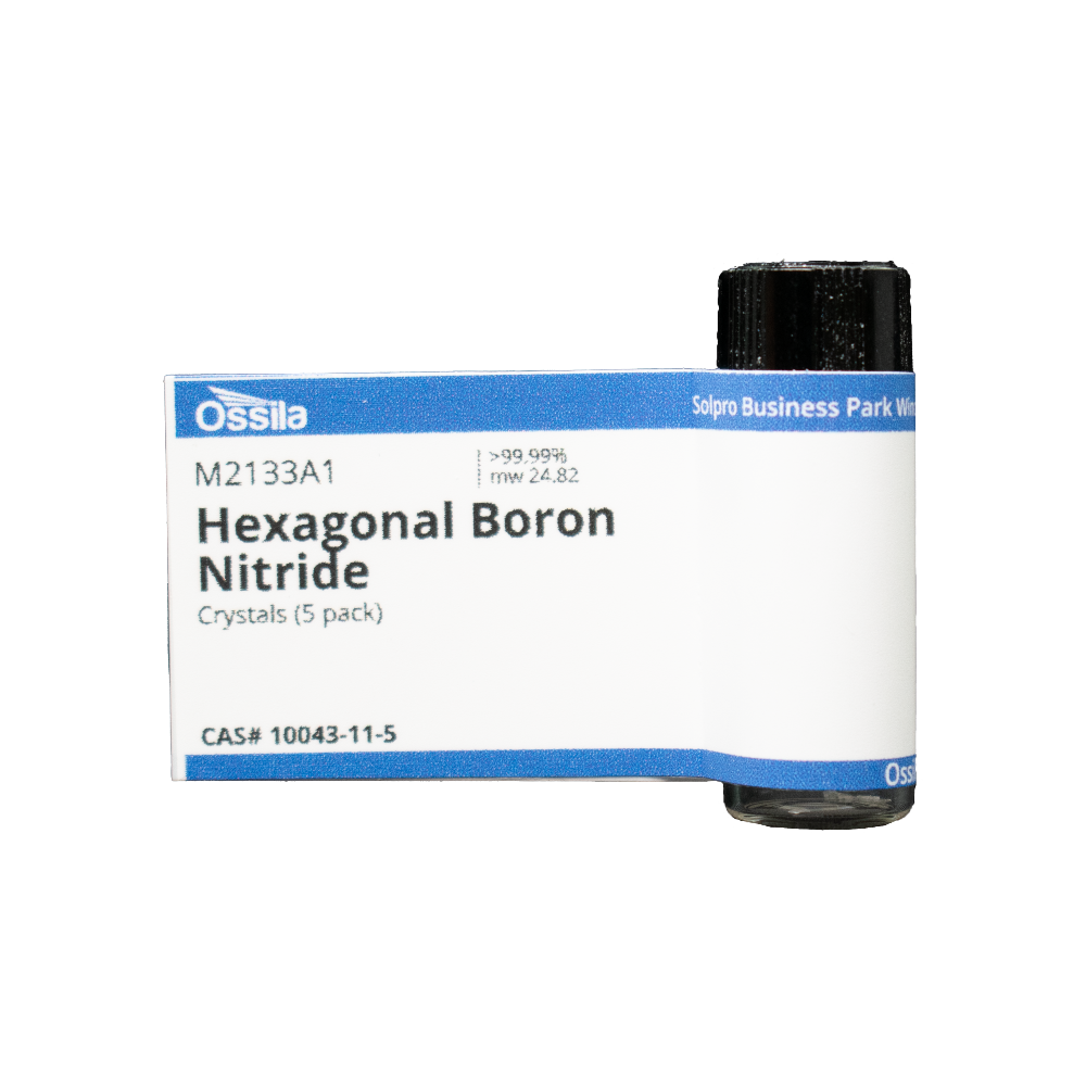
| M2133A1 | Crystals | Pack of 5 Crystals | £520 |
| M2133C1 | Crystals | Pack of 10 Crystals | £900 |
| M2161F11 | Monolayer Films | SiO2/Si - 1 Each | £200 |
| M2161F11 | Monolayer Films | SiO2/Si - 2 Each | £340 |
| M2162F11 | Monolayer Films | PET - 1 Each | £200 |
| M2162F11 | Monolayer Films | PET - 2 Each | £340 |
| M2319F11 | Monolayer Films | Sapphire - 1 Each | £200 |
| M2319F11 | Monolayer Films | Sapphire - 2 Each | £340 |
| M2320F11 | Monolayer Films | Quartz - 1 Each | £200 |
| M2320F11 | Monolayer Films | Quartz - 2 Each | £340 |
| M2163F11 | Few-Layer Films | SiO2/Si - 1 Each | £200 |
| M2163F11 | Few-Layer Films | SiO2/Si - 2 Each | £340 |
| M2164F11 | Few-Layer Films | PET - 1 Each | £200 |
| M2164F11 | Few-Layer Films | PET - 2 Each | £340 |
| M2321F11 | Few-Layer Films | Sapphire - 1 Each | £200 |
| M2321F11 | Few-Layer Films | Sapphire - 2 Each | £340 |
| M2322F11 | Few-Layer Films | Quartz - 1 Each | £200 |
| M2322F11 | Few-Layer Films | Quartz - 2 Each | £340 |
*typical representative size, areas/dimensions may vary
**item with a lead time of 4 - 6 weeks, please contact for more information
Shipping is free for qualifying orders.
MSDS Documents
Monolayer Film
 Hexagonal boron nitride monolayer film SiO2/Si
Hexagonal boron nitride monolayer film PET
Hexagonal boron nitride monolayer film sapphire
Hexagonal boron nitride monolayer film quartz
Few-Layer Film
Hexagonal boron nitride few-layer film SiO2/Si
Hexagonal boron nitride few-layer film PET
Hexagonal boron nitride few-layer film sapphire
Hexagonal boron nitride few-layer film quartz
Structure of Hexagonal Boron Nitride
With a honeycomb structure based on sp2 covalent bonds similar to graphene, hexagonal boron nitride is also known as “white graphene”. h-BN monolayers have a layered structure (again, very similar to graphene).
The hexagonal crystal structure of h-BN is one of the three crystalline forms of boron nitride (BN). BN crystallises in hexagonal form at room temperature and normal pressure. It is the most stable phase of the three crystalline forms. At higher temperature and pressure, h-BN transform into a wurtzite structure (P63mc).

Properties of Hexagonal Boron Nitride
After exfoliation of Hexagonal Boron Nitride crystal or powder, Hexagonal Boron Nitride typically has the following properties:
- Known as “white graphene”
- BN crystallises in hexagonal form (P63mc)
- Normally considered an insulator
- With an indirect bandgap (at 5.955 eV), and thus is also considered a semiconductor
Literature and Reviews
- Hexagonal boron nitride is an indirect bandgap semiconductor, G. Cassabois et al., Nat. Photon., 10, 262–266 (2016);DOI: 10.1038/NPHOTON.2015.277.
- Graphene, hexagonal boron nitride, and their heterostructures: properties and applications, J. Wang et al., RSC Adv., 7, 16801 (2017); DOI: 10.1039/c7ra00260b.
- Two dimensional hexagonal boron nitride (2D-h-BN): synthesis, properties and applications, K. Zhang et al., J. Mater. Chem. C, 5, 11992 (2017); DOI: 10.1039/c7tc04300g.