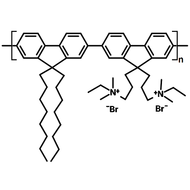
PFO (F8)
CAS Number 19456-48-5
OFET & OLED Polymer Materials, Perovskite Interface Materials, Perovskite Materials, Semiconducting Polymers
PFO, semiconducting polymer for high efficiency green OLEDs
High quality polymer available for fast, secure dispatch
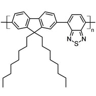
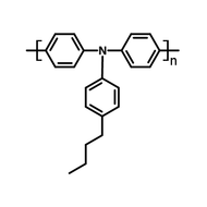
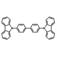
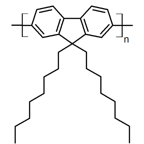
Poly(9,9-di-n-octylfluorenyl-2,7-diyl), known as F8 or PFO, is a polyfluorene specifically optimized for a variety of organic electronic applications.
General Information
| CAS Number | 19456-48-5 |
|---|---|
| Chemical Formula | (C29H41)n |
| Full Name | Poly(9,9-di-n-octylfluorenyl-2,7-diyl) |
| Recommended solvents | Toluene, xylene, chlorobenzene |
| Synonyms |
F8 PFO |
| Classification / Family | Polyfluorenes, Benzothiodiazoles, Organic semiconducting materials, Semiconducting polymers, OLED green emitter materials, OLED materials, Organic photovoltaic (OPV) materials, Polymer solar cells, OFET materials |
Chemical Structure

Characterization

Applications
For a high-efficiency green OLED we recommend blending F8 with F8BT with the below specifications. This ink can then be applied either in air, or in a glove box, with little difference in performance (provided exposure time and light levels are minimised). For more details see our fabrication guide.
At typical concentrations of 10 mg/ml, 100 mg of F8 (PFO) will make around 200 devices on Ossila's standard ITO substrates (20 x 15 mm), assuming 50% solution usage (50% loss in filtering and preparation).
OLED reference device:- F8 with F8BT
- Blend ratio of 19:1 (F8:F8BT) in Toluene
- Total concentration of 10 mg/ml
- 0.45 μm PTFE filter (hydrophobic)
- Spun at 2000 rpm (approx. 70 nm thickness)
Pipetting 20 μl of the above solutions onto a substrate spinning at 2000 rpm should provide a good even coverage, with approximately 70 nm thickness. The substrate needs to be spun until dry, which is typically only a few seconds — 15 seconds should be ample to achieve this. Thermal annealing should be undertaken at 80°C for 10 minutes prior to cathode deposition.
Typical Device Architectures and Performance
A basic, efficient OLED can be made using PEDOT:PSS as a hole-transport layer and Calcium/Aluminum as the electron contact. When used with the Ossila ITO glass OLED substrates and shadow masks this produces an easy to fabricate yet efficient >100 cd/m2 device.

MSDS Documentation
 PFO (F8) MSDS sheet
Batch Details
| Batch number | MW | MN | PDI | Stock info |
|---|---|---|---|---|
| M161 | 114,050 | 37,910 | 3.00 | Discontinued |
| M162 | 85,983 | 31,040 | 2.77 | Discontinued |
| M163 | 57,798 | 21,328 | 2.71 | Discontinued |
| M164 | 63,114 | 19,125 | 3.30 | Discontinued |
| M0161A1 | 105,491 | 45,275 | 2.33 | Discontinued |
| M0161A2 | 77,293 | 29,167 | 2.65 | Discontinued |
| M0161A3 | 260,817 | 93,709 | 2.78 | In stock |
Related Products
We stock a wide range of perovskite interface materials. Please contact us if you cannot find what you are looking for.