ITO Glass Substrates, 25 mm Square, PV and OLED
Patterned ITO substrates for rapid prototyping.
Large pixels for record breaking-devices.
The patterned Indium Tin Oxide (ITO) Glass subtrates are part of Ossila's award winning prototyping platform. ITO is both conductive and transparent, which makes it an ideal material for use with optoelectronic devices such as photovoltaics and OLEDs.

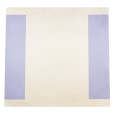
As thin film technology improves, the active areas of device pixels increase in size. The 25mm square substrates have been designed to help the community take the next step in scaling up active areas. When combined with our desposition masks, these substrates allow four pixels per substrate, with active areas of 48mm2 each.
The following video shows the fabrication and testing of devices using the PV and OLED device prototyping substrate system and a glove box.
| Substrate size | 25 mm x 25 mm |
| Thickness | 1.1 mm |
| Glass type | Polished soda lime, float glass |
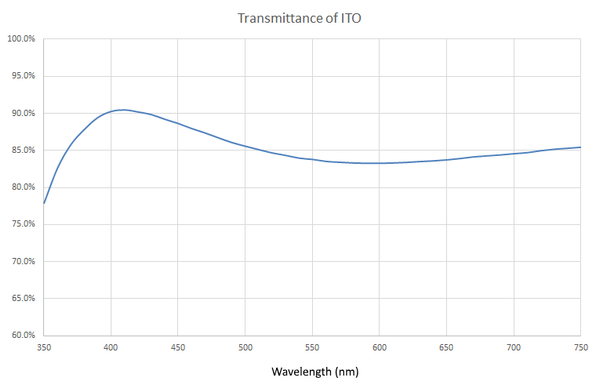
| Substrate coating | Fully oxidized ITO |
| ITO thickness | 100 nm |
| ITO resistance | 20 Ω / square |
| Glass roughness | < 1 nm RMS (By AFM) |
| ITO roughness | 1.8 nm RMS (By AFM) |
| Pixel Sizes | 48 mm2 (6 mm x 8 mm) |