
Deposition Masks, 20 x 15 mm
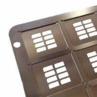
Ossila have produced a range of masks for vacuum deposition of materials onto our standardised 8-pixel substrate design. These include masks that are used to deposit electrodes and busbars and masks to deposit semiconducting materials to define an active area for thin film electronic devices - all to obtain the highest device performances possible. All our deposition masks are made from stainless steel, with the option of an additional spacer layer.
Looking for generation I (E114/5/6, E631) or II (E345/6, E355/6) deposition masks for S101 or S171 substrates?
We have discontinued our generation I and generation II substrates and masks. The replacement 8-pixel design allows you to create either eight small individual pixels or a single large pixel. Contact us for more information, technical support and advice, or for help migrating to the new system.
We provide the following masks that are suitable for use with our S211 substrate design:
- Busbar mask - Allows for the deposition of high conductivity metals on non-critical parts of the ITO to reduce resistive losses within devices
- Active material masks - Defines an area for the deposition of the materials you wish to study
- Multi electrode masks - Defines a pattern for the deposition of 8 electrodes producing 8 complete devices upon a single substrate, each device has an active area of 4mm2
- Single electrode masks - Defines a single large electrode across the center of the substrate producing a device with an active area of 48mm2
- Multi electrode/busbar masks - A combination of the multi electrode and the busbar mask, allowing for the deposition of 8 individual electrodes and the coating of non-critical parts of the ITO.

Spacer Layers
Each mask has the option of the addition of a 100 µm spacer layer that can be placed between the mask and the substrate. This spacer layer reduces the direct contact between the surface of the substrate and the mask by over 98%. This is recommended for samples that are easily scratched or for porous samples that experience a large amount of out-gassing. For sputtering or other non-directional deposition techniques, the spacer layer is not recommended as the presence of a spacer layer will reduce the precision of your deposited edge.
Deposition Mask Specifications and Designs
General Specifications
| Material | Stainless Steel |
| Outer Dimensions | 75mm x 75mm |
| Substrate Recesses | 12 |
| Recess Dimensions | 20.15mm x 15.15mm |
| Thickness | 1.7mm without spacer, 1.8mm with spacer (E504: 1.6mm without spacer, 1.7mm with spacer)(exc. bolts) |
Busbar Mask

Ossila's busbar mask has been designed to eliminate resistance losses that occur when using transparent conductive layers. By allowing for the deposition of high conductivity metals across non-critical parts of the transparent conductor the overall resistive losses that occur within thin film electronic devices can be reduced. The busbar mask should be used before any other layers are deposited onto your S211 substrate. The deposition pattern overlaid onto our S211 substrate is shown to the right.
The schematic drawing of our busbar mask can be seen below.

Active Material Mask

Ossila's active material mask is specifically designed to coat the areas where your electrodes will be overlapping. The range of materials and techniques that can be used is nearly endless; whether it is vacuum deposited small molecules, chemical vapor deposition of ceramics, or sputtering of metallic alloys, the active material mask will allow you to accurately define your deposition area. The deposition pattern overlaid onto our S211 substrate is shown to the right.
The schematic drawing of our active material mask can be seen below.
Multi-Electrode Mask

Ossila's multi-electrode mask has been designed to obtain the most amount of pixels from a single substrate. Using our multi-electrode mask, it is possible to define 8 x 4mm2 devices. In addition, by placing the electrodes in the middle of the substrate edge defects from solution processing of films can be eliminated improving the reliability of devices across a substrate. By using a multi-electrode structure, device statistics are significantly improved -- allowing you to feel confident in the results you are obtaining from thin film device fabrications. The deposition pattern overlaid onto our S211 substrate is shown to the right.
The schematic drawing of our multi electrode mask can be seen below:
Single-Electrode Mask

Ossila's single electrode mask has been designed to give the largest area for a device using our S211 substrate. Using our single-electrode mask, it is possible to define a 48mm2 device. By looking at large single-electrode devices, it is possible to study the changes in performance of thin film devices when transitioning from small scale lab devices to large scale industrial processes. The deposition pattern overlaid onto our S211 substrate is shown to the right.
The schematic drawing of our single electrode mask can be seen below:
Multi-Electrode/Busbar Mask
Ossila's multi-electrode busbar mask has been designed to obtain the highest performance whilst maintaining a minimum amount of deposition steps. Using a combination of our multi-electrode mask and busbar mask, 8 electrodes can be defined whilst allowing for the deposition of extra material to reduce resistive losses. By using our multi-electrode/busbar mask, the best device performance can be achieved whilst maintaining the same amount of fabrication steps as our regular multi-electrode mask. The deposition pattern overlaid onto our S211 substrate is shown to the right.
The schematic drawing of our multi-electrode/busbar mask can be seen below:

TCO Pattern Mask
Ossila's TCO Pattern mask can be used to replicate the pattern of the ITO on our S211 substrates.
The schematic drawing of our TCO pattern mask can be seen below:
