Black Phosphorus
Black phosphorus was first synthesised in 1914 by Percy W Bridgman by heating white phosphorus at high pressures. It is the most stable known allotrope of phosphorus and consists of 2-dimensional layers of phosphorus, known as phosphorene.
Despite being largely overlooked for 100 years, the current boom in 2D materials research has resulted in black phosphorus gaining more attention. The individual phosphorene monolayers were first separated and studied in 2014, and research into the its unique properties and wide range of potential applications has been ongoing since. Within research, glove boxes are used to prevent degradation of its unique properties.
Browse Black Phosphorus

Black Phosphorus Powder
Can be used for preparation of black phosphorus quantum dots, nano-platelets and thin films. Available in quantities of 250 mg, 500 mg, or 1 g with ≥99.995% purity.
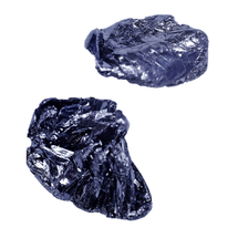
Black Phosphorus Crystal
Can be used to produce single or few-layer phosphorene sheets via mechanical or liquid exfoliation. Small or bulk crystal quantities available with ≥99.999% purity.
*Typical representative size, areas/dimensions may vary
Resources and Support
 What is Black Phosphorus?
Black phosphorus is a crystalline allotrope of phosphorus. It is distinct from the more common white and red forms of phosphorous due to its unique structure and properties.
Read more... Black Phosphorus Uses and Applications
Due to the unique properties, exfoliated monolayer and few-layer black phosphorus have potential for a wide range of applications in electronics and optoelectronics.
Read more... Black Phosphorus Structure
Black phosphorus has gained attention for its distinct structural properties when reduced to two-dimensional layers known as phosphorene.
Read more...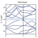 Black Phosphorus Properties
The optical, electronic, and mechanical properties of phosphorene differ from that of the bulk state due to combinations of factors.
Read more... The Allotropes of Phosphorus
Depending on environmental conditions and how it is processed, elemental phosphorus can take several forms: white, red, black, and violet phosphorus.
Read more...Literature and Reviews
- The renaissance of black phosphorus, X. Ling et al., PANS, 112 (15), 4523-4530 (2015); DOI: 10.1073/pnas.1416581112.
- Isolation and characterization of few-layer black phosphorus, A. Castellanos-Gomez et al., 2D Mater. 1(2) 025001 (2014); doi:10.1088/2053-1583/1/2/025001.
- High-mobility transport anisotropy and linear dichroism in few-layer black phosphorus, J. Qiao et al., Nat. Commun., 5:4475 (2014); DOI: 10.1038/ncomms5475.
- Black Phosphorus: Narrow Gap, Wide Applications, A. Castellanos-Gomez, J. Phys. Chem. Lett., 6, 4280−4291 (2015); DOI: 10.1021/acs.jpclett.5b01686.
- Strain Engineering for Phosphorene: The Potential Application as a Photocatalyst, B.Sa et al., J. Phys. Chem. C, 118 (46), 26560–26568 (2014); DOI: 10.1021/jp508618t.
- Phosphorene: Fabrication, Properties, and Applications, L. Kou etal., J. Phys. Chem. Lett., 2015, 6 (14), 2794–2805 (2015); DOI: 10.1021/acs.jpclett.5b01094
- Strain-Engineering the Anisotropic Electrical Conductance of Few-Layer Black Phosphorus, R. Fei et al., Nano Lett., 14 (5), 2884–2889 (2014); DOI: 10.1021/nl500935z.
- Layer-dependent Band Alignment and Work Function of Few-Layer Phosphorene, Y. Cai et al., Sci. Rep., 4 : 6677 (2014); DOI: 10.1038/srep06677.
- Visualizing Optical Phase Anisotropy in Black Phosphorus, S. Lan et al., ACS Photonics, 3 (7), 1176–1181 (2016); DOI: 10.1021/acsphotonics.6b00320.
- Recent advances in synthesis, properties, and applications of phosphorene, M. Akhtar et al., NPJ 2D Mater. Appl., 1, 5 (2017).
- Semiconducting Black Phosphorus, A. Morita, Appl. Phys. A 39, 227-242 (1986)
- Black Phosphorus Gas Sensors, A. Abbas et al., ACS Nano, 9 (5), 5618–5624 (2015)
- Semiconducting black phosphorus: synthesis, transport properties and electronic applications, H. Liu et al., Chem. Soc. Rev., 44, 2732 (2015)
- From Black Phosphorus to Phosphorene: Basic Solvent Exfoliation, Evolution of Raman Scattering, and Applications to Ultrafast Photonics, Z. Guo et al., Adv. Funct. Mater., 25, 6996–7002 (2015)
- High-quality sandwiched black phosphorus heterostructure and its quantum oscillations, X. Chen et al., Nat. Commun., 6, 7315 (2015)
- Anisotropic in-plane thermal conductivity observed in few-layer black phosphorus, Z. Luo et al., Nat. Commun., 6, 8572 (2015)
- Phosphorene: An Unexplored 2D Semiconductor with a High Hole Mobility, H. Liu et al., ACS Nano, 8 (4), 4033–4041 (2014)
- Black Phosphorus-Monolayer MoS2 van der Waals Heterojunction p-n Diode, Y. Deng et al., ACS Nano, 8 (8), 8292–8299 (2014)
- Two-dimensional crystals: Phosphorus joins the family, Nat. Nanotech., 9 (5), 330 (2014)
- Black Phosphorus Quantum Dots with Tunable Memory Properties and Multilevel Resistive Switching Characteristics, S. Han et al., Adv. Sci., 4, 1600435 (2017); DOI: 10.1002/advs.201600435.
- Quantum dots derived from two-dimensional materials and their applications for catalysis and energy, X, Wang et al., Chem. Soc. Rev., 45, 2239 (2016); DOI: 10.1039/c5cs00811e.
- Electronic properties of bilayer phosphorene quantum dots in the presence of perpendicular electric and magnetic fields, L. Li et al., Phys. Rev. B 96, 155425 (2017); DOI: 10.1103/PhysRevB.96.155425.
- Black Phosphorus Quantum Dots, X. Zhang et al., Angew. Chem. Int. Ed., 54, 3653 –3657 (2015); DOI: 10.1002/anie.201409400.
- Ultrasmall Black Phosphorus Quantum Dots: Synthesis and Use as Photothermal Agents, Z. Sun et al., Angew. Chem., 127,11688 –11692 (2015); DOI:10.1002/ange.201506154.
- Red Phosphorus: An Elemental Photocatalyst for Hydrogen Formation from Water, F. Wang et al., Appl. Catal., 111, 409-414 (2012)
- Single-Layered Hittorf’s Phosphorus: A Wide-Bandgap High Mobility 2D Material, Schusteritsch et al., Nano Lett., 16 (5), 2975-2980 (2016)
- 2D Nanoelectronics: Physics and Devices of Atomically Thin Materials, M. Dragoman and D. Dragoman, Springer International Publishing (2017)
- Thermal conductivity determination of suspended mono- and bilayer WS2 by Raman spectroscopy, Peimyoo et al., Nano Research, 8 (4), 1210–1221 (2015)
- Thermal Conductivity of Monolayer Molybdenum Disulfide Obtained from Temperature-Dependent Raman Spectroscopy, R. Yan et al., ACS Nano, 8 (1), 986–993 (2014)
- Black phosphorus field-effect transistors, Li et al, Nature Nanotechnology, 9, 372–377 (2014)
- Anisotropic Thermal Conductivity of Exfoliated Black Phosphorus, H. Jang et al., Advanced materials, 27 (48), 8017-8022 (2015)
- Rediscovering black phosphorus as an anisotropic layered material for optoelectronics and electronics, Xia et al., Nature Communications, 5, 4458 (2014)
- Graphene Field-Effect Transistors with High On/Off Current Ratio and Large Transport Band Gap at Room Temperature, F. Xia et al., Nano Lett., 10 (2), 715–718 (2010)
- High-mobility and air-stable single-layer WS2 field-effect transistors sandwiched between chemical vapor deposition-grown hexagonal BN films, M. Iqbal et al., Scientific Reports, 5, 10699 (2015)
- Low voltage and high ON/OFF ratio field-effect transistors based on CVD MoS2 and ultra high-k gate dielectric PZT, C. Zhou et al., Nanoscale, 7, 8695-8700 (2015)
- Optical tuning of exciton and trion emissions in monolayer phosphorene, J. Yang et al., Light: Science & Applications, 4, 312 (2015)
- Tin Disulfide-An Emerging Layered Metal Dichalcogenide Semiconductor: Materials Properties and Device Characteristics, Y. Huang et al., ACS Nano, 8 (10), 10743–10755 (2014)
- SnS-based thin film solar cells: perspectives over the last 25 years, Journal of Materials Science: Materials in Electronics, J. Andrade-Arvizu et al., 26 (7), 4541–4556 (2015)
- Tin(II) Sulfide (SnS) Nanosheets by Liquid-Phase Exfoliation of Herzenbergite: IV−VI Main Group Two-Dimensional Atomic Crystals, J. Brent et al., J. Soc., 137, 12689 (2015)
- Tuning magnetotransport in a compensated semimetal at the atomic scale, L. Wang et al., Nature Communications, 6, 8892 (2015)
- Tungsten ditelluride: a layered semimetal, C. Lee, Scientific Reports, 5, 10013 (2015)
- Indirect-to-Direct Band Gap Crossover in Few-Layer MoTe2, I. Lezama, Nano Lett., 15 (4), 2336-2342 (2015)
- Optical Properties and Band Gap of Single- and Few-Layer MoTe2 Crystals, C. Ruppert et al., Nano Lett., 14 (11), 6231-6236 (2014)
- Black Phosphorus Photodetector for Multispectral, High-Resolution Imaging, M. Engel et al., Nano Lett, 14 (11), 6414–6417 (2014)
- Waveguide-integrated black phosphorus photodetector with high responsivity and low dark current, N. Youngblood et al., Nature Photonics, 9, 247–252 (2015)
- Fast and Broadband Photoresponse of Few-Layer Black Phosphorus Field-Effect Transistors, M. Buscema et al., Nano Lett., 14 (6), 3347–3352 (2015)
- Photovoltaic effect in few-layer black phosphorus PN junctions defined by local electrostatic gating, M. Buscema et al., Nature Communications, 5, 4651 (2014)
- Edge-Modified Phosphorene Nanoflake Heterojunctions as Highly Efficient Solar Cells, W. Hu et al., Nano Lett., 16 (3), 1675–1682 (2016)
- Ultrahigh sensitivity and layer-dependent sensing performance of phosphorene-based gas sensors, S. Cui et al., Nature Communications, 6, 8632 (2015)
- Large Electronic Anisotropy and Enhanced Chemical Activity of Highly Rippled Phosphorene, A. Kistanov et al., Phys. Chem. C, 120 (12), 6876–6884 (2016)
- Ultrafast and Directional Diffusion of Lithium in Phosphorene for High-Performance Lithium-Ion Battery, W. Li et al., Nano Lett., 15 (3), 1691–1697 (2015)
- Phosphorene as an anode material for Na-ion batteries: a first-principles study, V. Kulish et al., Phys. Chem. Chem. Phys., 17, 13921-13928 (2015)
- Growth of 2D black phosphorus film from chemical vapor deposition, J. Smith et al., Nanotechnology, 27 (21), 215602 (2016)