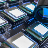
Photovoltaic Substrate (8 Pixel) - Overview and Schematic

Ossila's photovoltaic substrates have been developed to maximize performance and fabrication efficiency for a range of modern photovoltaic device types where ITO series resistance becomes critical.
Developed and evolved over a number of years, these substrates have become the mainstay of our own research on organic photovoltaics and perovskite PV but are also used by customers around the world for a wide array of device types including:
- Perovskite solar cells
- Bulk heterojunction (solution processed) organic photovoltaics (OPV)
- Planar heterojunction (vacuum processed) organic photovoltaics (OPV)
- Copper Indium Gallium Selenide (CIGS) solar cells
- Copper Zinc Tin Sulfide (CZTS) solar cells
- Quantum dot solar cells
System Overview
The below diagrams show schematically how devices are built on the photovoltaic substrate. There are also many variations of these architectures that can be built using the same substrate but below we have outlined the most common.
Step 1: Clean
Clean the ITO coated substrate using an electronic grade cleaning agent (such as Hellmanex) and organic wash routine to remove any surface particulates. Then ensure the surface is chemically clean and hydrophobic by using either sonication in a strong base such as NaOH or by using a UV Ozone cleaner.

Step 2: Deposit Interlayer
Deposit the hole transport layer (or electron transport layer if building inverted devices). If using solution processed layers such as PEDOT:PSS or ZnO solgels then this is typically done by spin coating, blade coating or spray coating followed by wiping the edges clean but a cleanroom swab. If using vacuum deposition interlayers such as MoOx or BCP then this can be done by using our active area deposition mask.

Step 3: Deposit Active Layer
This can be done in the same way as step 2 above. However, if both layers are solution processed then care needs to be taken to ensure that orthogonal solvents are used so that the bottom layer isn't washed away when depositing the top layer. For help choosing orthogonal solvents, contact our technical team.

Step 4: Deposit the top cathode (and any additional interlayers)
For non-inverted devices the top electrode (sometimes called the back contact) is often a combination of an electron interface such as calcium, LiF, C60 or BCP with a highly conductive overlayer (aluminum or silver). For inverted devices this is an hole interface such as MoOx with again a conductive back contact such as aluminum, silver or gold.
The same substrate can also be used with two different pixel arrangements just by changing the shadow mask. This can result in either eight small pixels for maximum statistical data or one large pixel for maximum area.


As an alternative to vacuum processing, solution processed top cathodes can also be used such as the HTL Solar PEDOT:PSS formulation.
Step 5: Encapsulate
The Ossila encapsulation epoxy can be used safely with a wide range of delicate or reactive materials from polymers to calcium and in conjunction with a glass coverslip provides hermetic encapsulation from the top and thereby can provide high lifetimes (up to 14,000 OPV lifetime in our labs).

Step 6: Measure
For any lab based devices the active area of the substrates is one of the primary sources of uncertainty. However, by using an electrochemically etched aperture mask which has dimensional aperture tolerance of less than 10 microns this uncertainty can be significantly reduced.

It's possible to connect to the substrates in a variety of ways such as using electrical connection legs (or even crocodile clips). However, to make life easy we also provide push-fit test boards which can be mounted to an optical bench underneath the solar simulator to allow quick and simple measurements.
Optional Steps
Add a bus bar
For any photovoltaic device the resistive loss scales with the current squared. As such, with modern thin films materials pushing current densities of over 20 mA/cm2 this can lead to nearly four times the resistive losses of older generation materials which could be up to a 5% of relative performance (up to 1% absolute power conversion efficiency for a 20% efficient device). To see details of these calculations see our photovoltaic resistive-losses white paper.
While the loss of a few percent may not make a huge difference when testing new materials on a day-to-day basis, when trying to get the best data you can for publication every little helps. Simply by adding a bus bar to the device it's possible to eliminate any unnecessary losses and can be deposited after cleaning with an additional evaporation of typically gold or silver using our photovoltaic substrate bus-bar mask (contact us for a quotation for this mask).

Substrates and Fabrication

Learn More
 Organic Solar Cells: An Introduction to Organic Photovoltaics
Organic solar cells, also known as photovoltaics (OPVs), have become widely recognized for their many promising qualities. This page introduces the topic of OPVs, how they work and their development.
Read more... Solar Cells: A Guide to Theory and Measurement
A solar cell is a device that converts light into electricity via the ‘photovoltaic effect’. They are also commonly called ‘photovoltaic cells’ after this phenomenon, and also to differentiate them from solar thermal devices. The photovoltaic effect is a process that occurs in some semiconducting materials, such as silicon.
Read more...